SemiconductorFab Design Engineering & Construction Summit
Facilities, utilities and capex delivery for multi-billion-dollar projects
The 7th Semiconductor Fab Design, Engineering & Construction APAC in Singapore is a dedicated forum for professionals responsible for planning, designing, building and expanding semiconductor fabs and advanced packaging facilities across Asia-Pacific. The summit focuses on facilities, utilities and CAPEX delivery for front-end fabs, OSAT and advanced packaging projects, rather than semiconductor technology itself.
As APAC leads global semiconductor investment, project teams face increasing challenges related to power supply, water and wastewater management, cleanrooms, vibration control, and complex construction delivery. Over two days, senior leaders from fabs, foundries, IDMs, memory manufacturers and OSATs will share practical lessons from projects across Singapore, Taiwan, Korea, Japan, Southeast Asia and India.
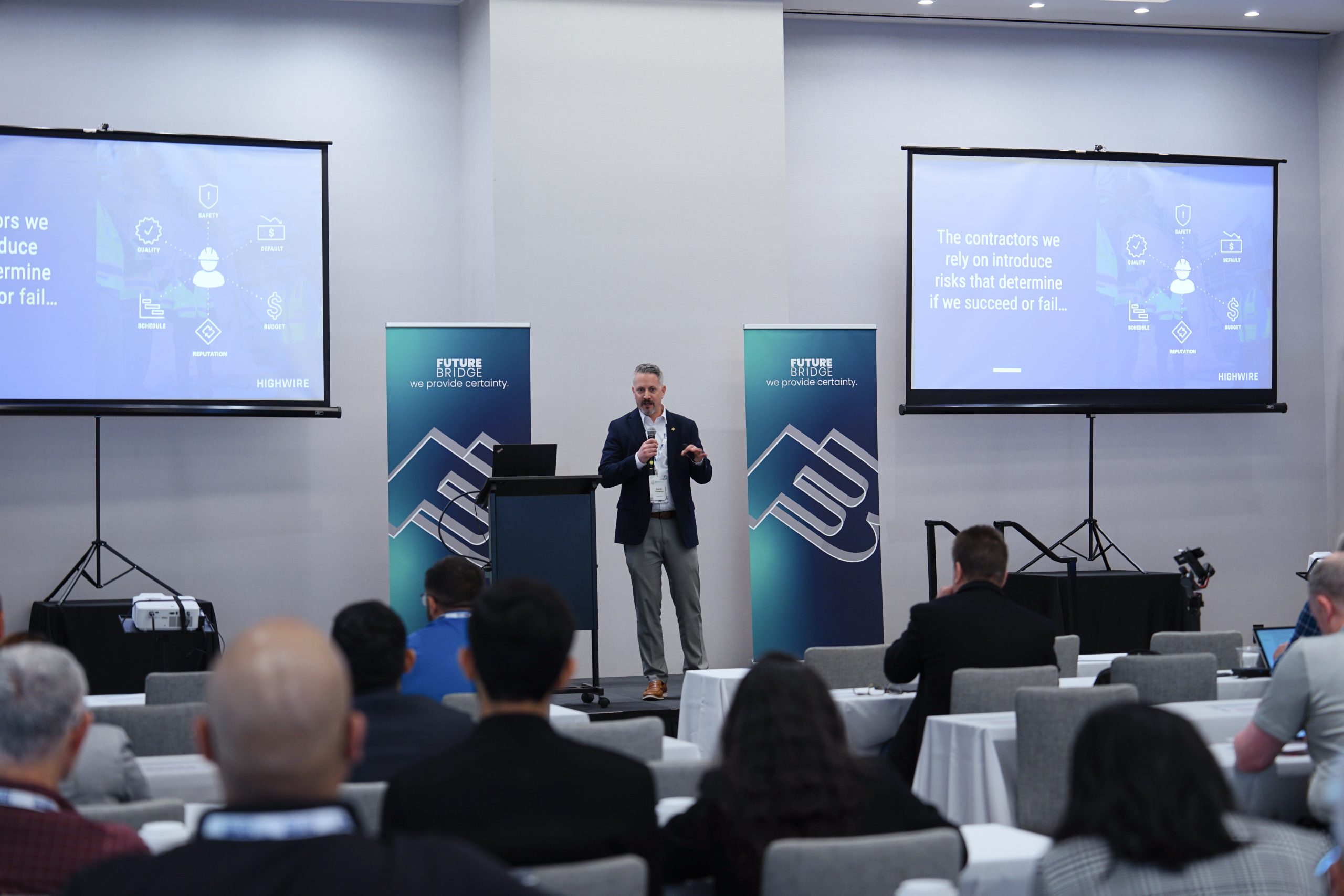
Industry experts from EPCs, cleanroom and MEP engineering, utilities, infrastructure and digital construction will present real-world case studies on modular construction, BIM/VDC, digital twins and innovative project delivery strategies that help reduce risk, accelerate project execution and build future-ready semiconductor manufacturing facilities.
Topics to be discussed
Comprehensive coverage of the most critical challenges and innovations shaping semiconductor facility design, construction and operations.
Mega-Fab construction and project delivery excellence
Advanced packaging facilities: engineering the next manufacturing frontier
High-NA EUV readiness: preparing fabs for the next generation of lithography
Overcoming construction bottlenecks in semiconductor expansion projects
Critical materials and supply chain assurance
Building the semiconductor workforce of tomorrow
Cost control and capital project optimisation
Advanced HVAC and cleanroom environmental control
Optimising humidity control for yield and process stability
Power infrastructure and grid readiness for high-density manufacturing
Certification, compliance and regulatory readiness
Risk management and mitigation across semiconductor capital projects
Integrating next-generation manufacturing equipment
Ultra-pure water systems and critical utility infrastructure
Five engineering pillars
The technical backbone of the two-day agenda. Choose a pillar to see what it covers.
Power, Utilities & Energy Architecture
For high-density fabs
- High-MVA grid connections and substation engineering
- Backup, resilience and onsite power systems
- Subfab utilities and critical infrastructure integration
Water, UPW, Wastewater & Environmental Systems
Capacity, reuse and compliance
- UPW plant design for next-generation nodes and packaging
- High-efficiency wastewater treatment and reuse
- Site sustainability and environmental compliance
Cleanroom, Building & Structural Engineering
For advanced fabs
- Cleanroom architecture and environmental control
- Vibration, EMI and noise mitigation for sensitive tools
- Brownfield upgrades and structural future-proofing
Construction, Modularization & Digital Delivery
Speed, predictability and control
- Modular construction and prefabrication for speed
- Land-constrained fab planning and vertical site utilization
- Fast-track delivery models for mega-projects
Site Selection, Expansion & Industrial Infrastructure
Brownfield strategy across APAC
- Engineering site readiness across APAC
- Brownfield capacity expansion without disruption
- Industrial park coordination and shared services
Trusted by industry partners
Ample networking throughout the two days
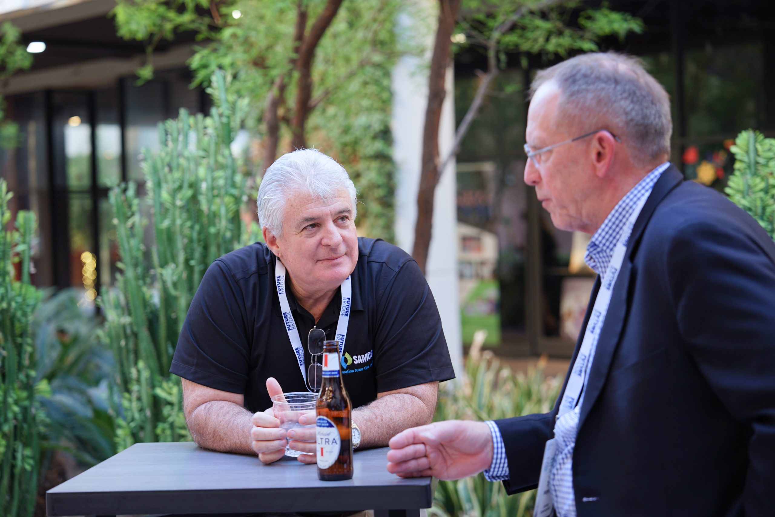
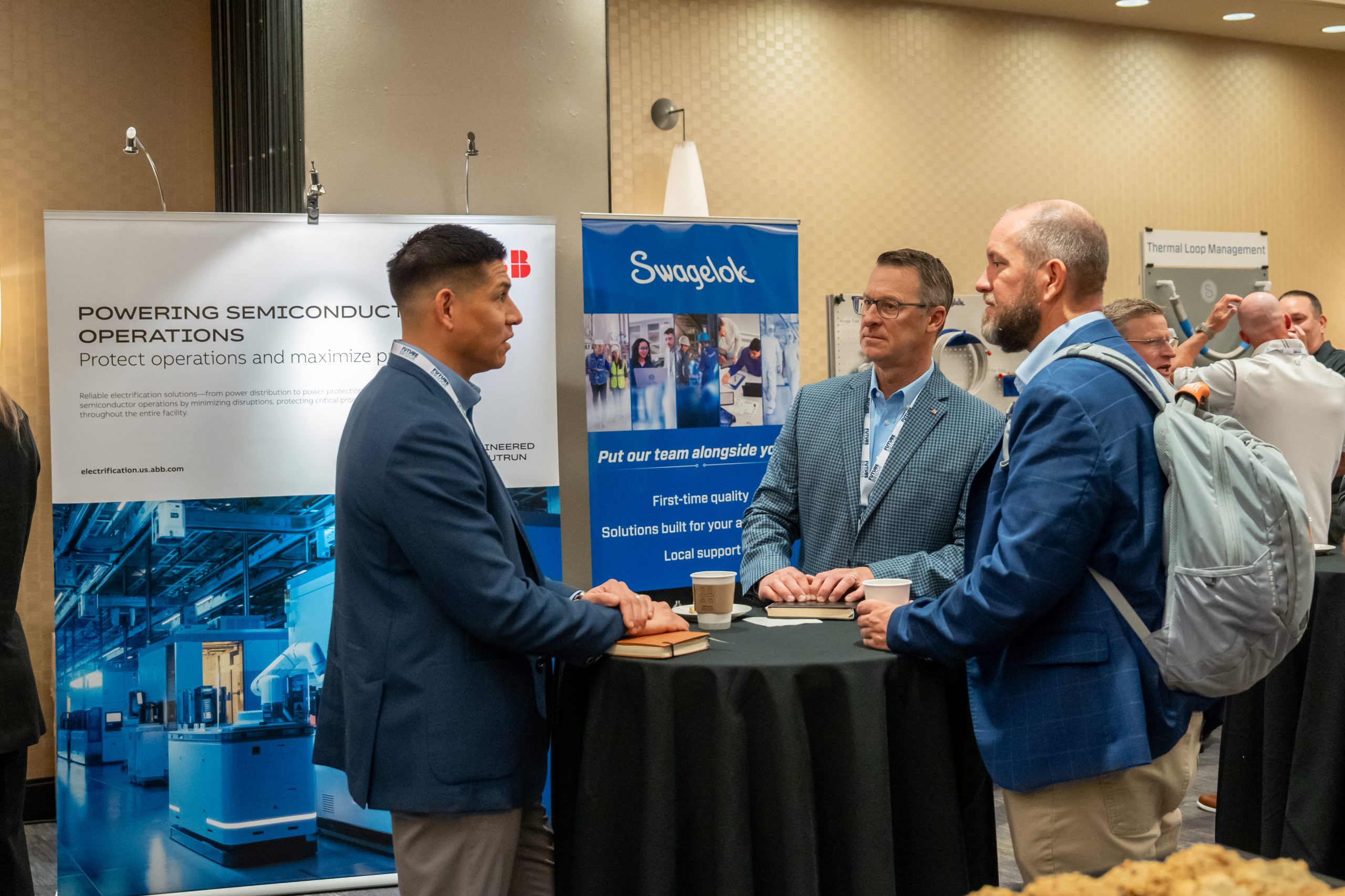
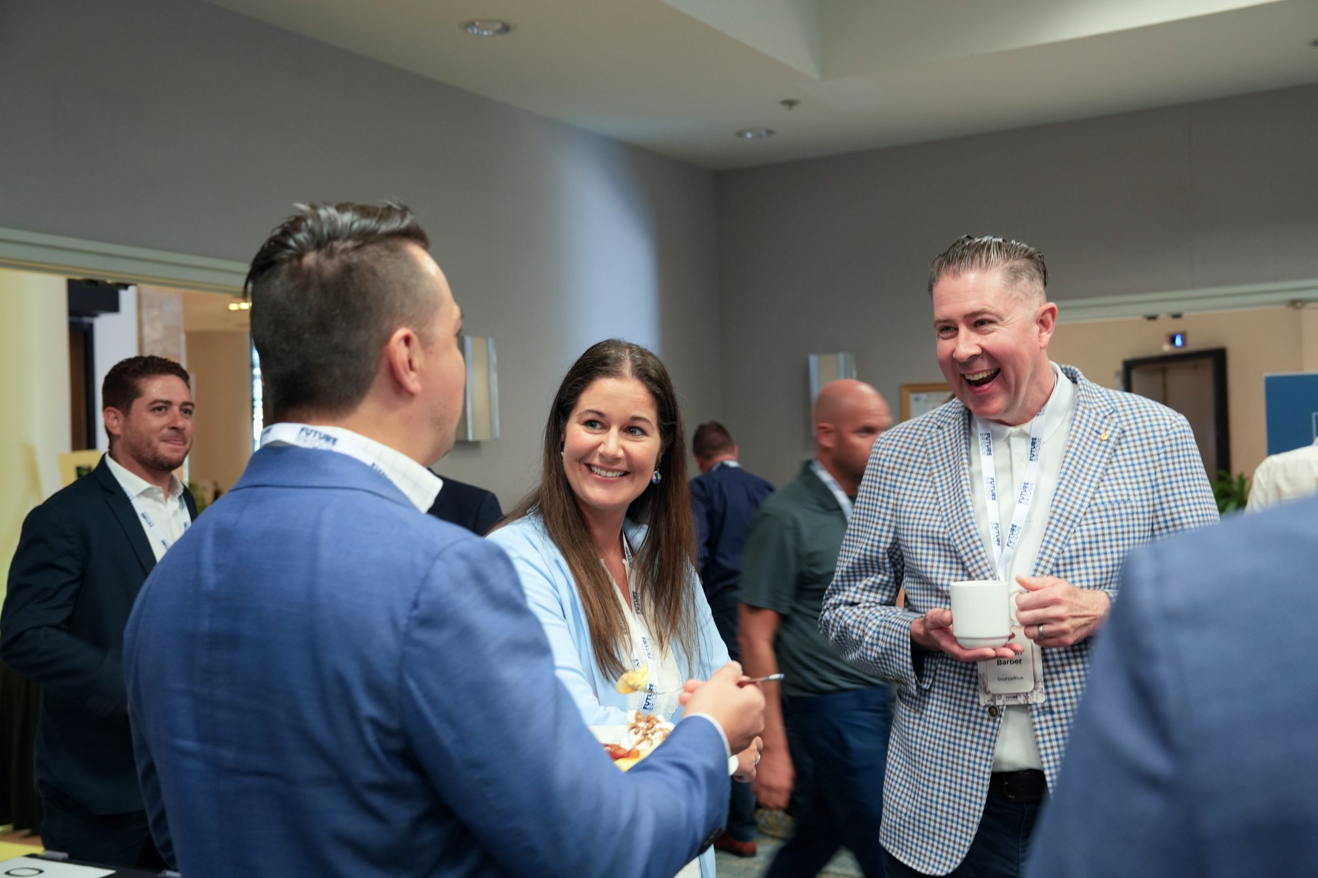
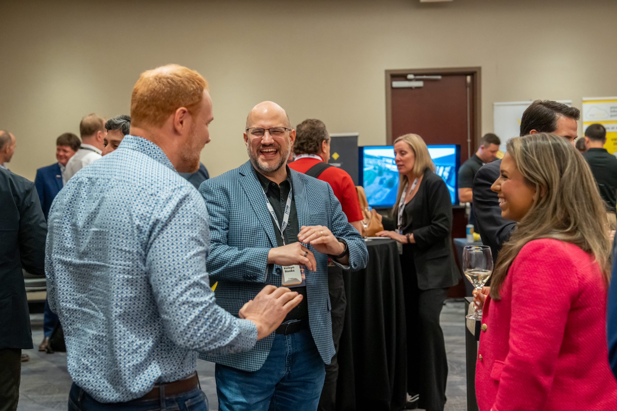
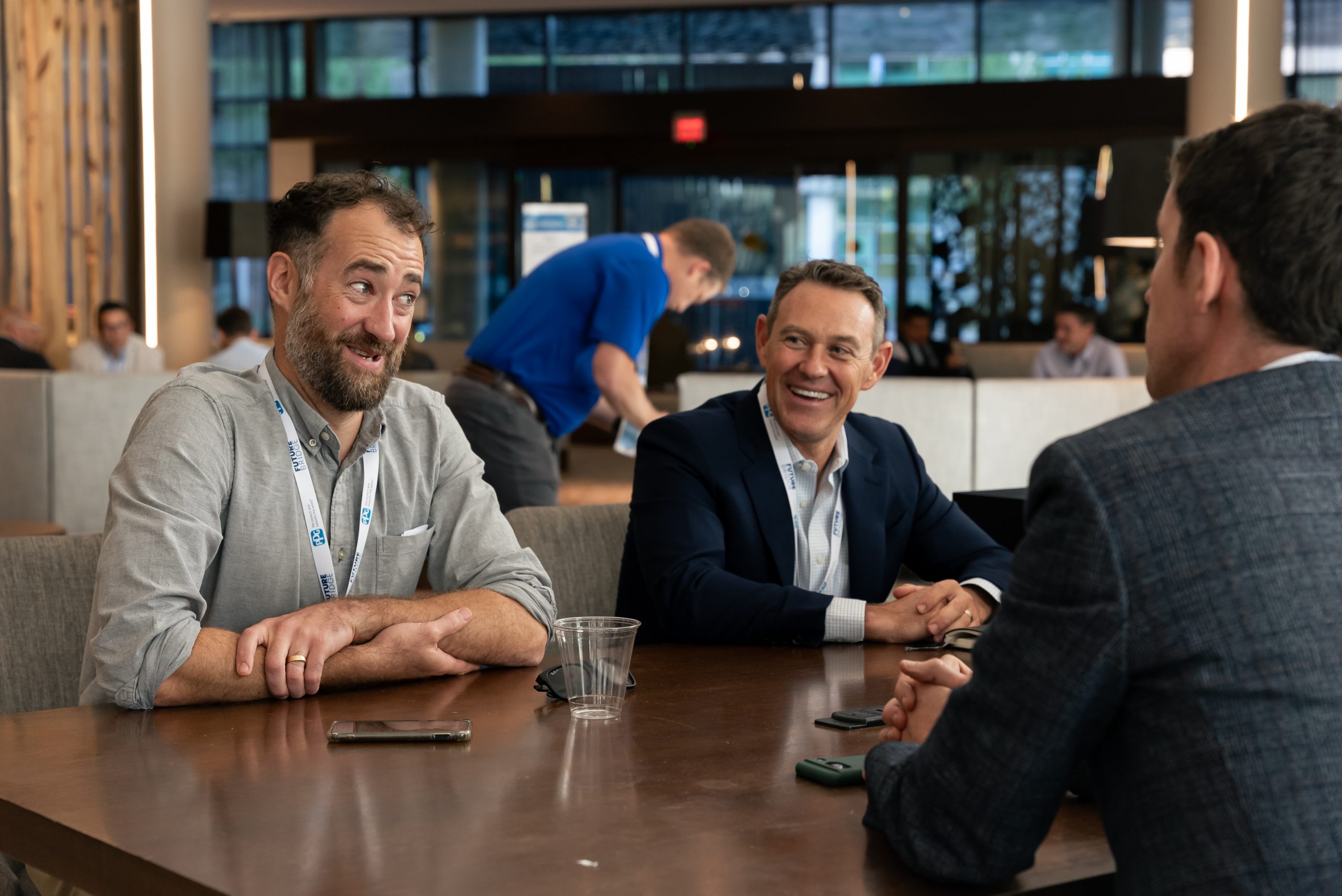
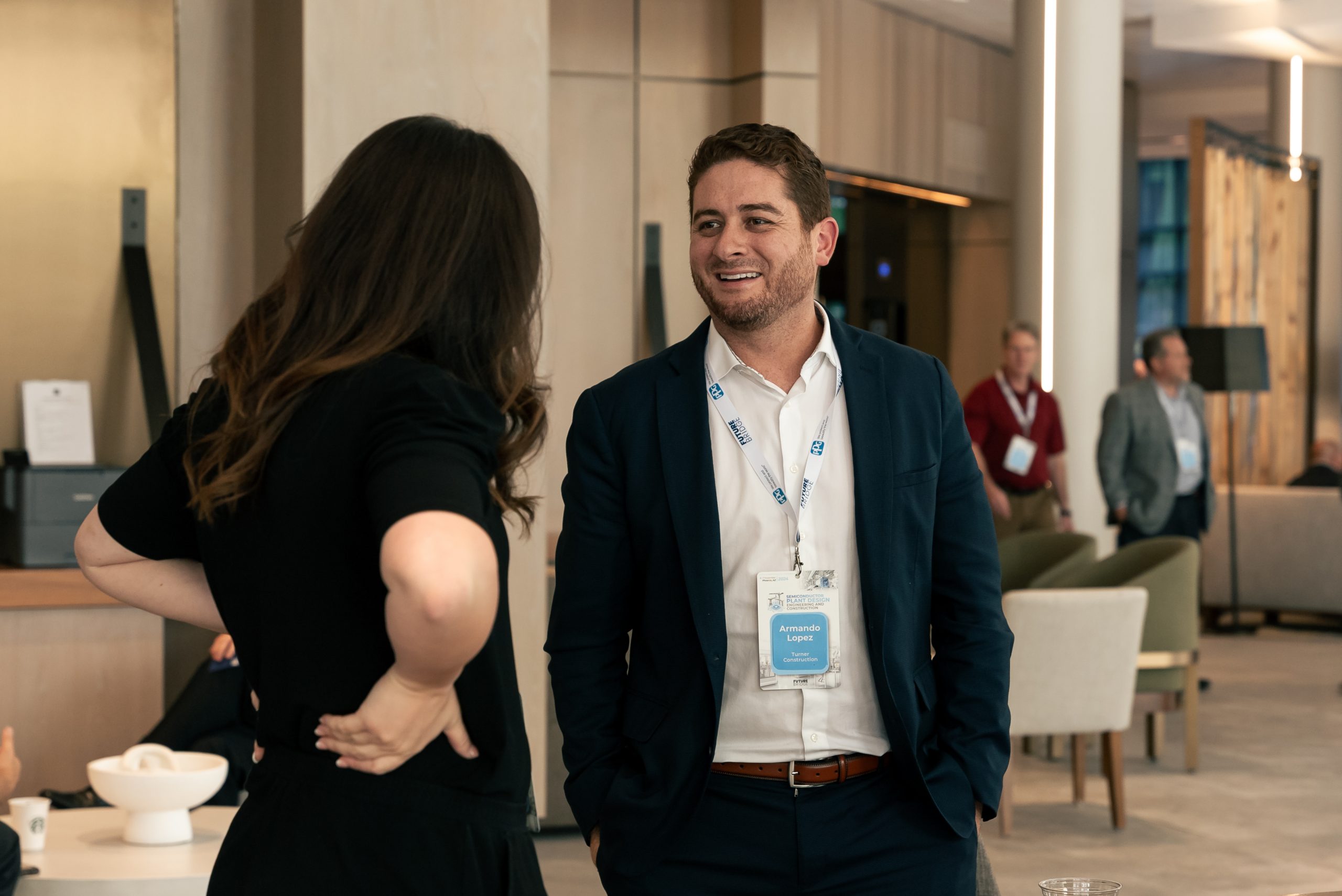
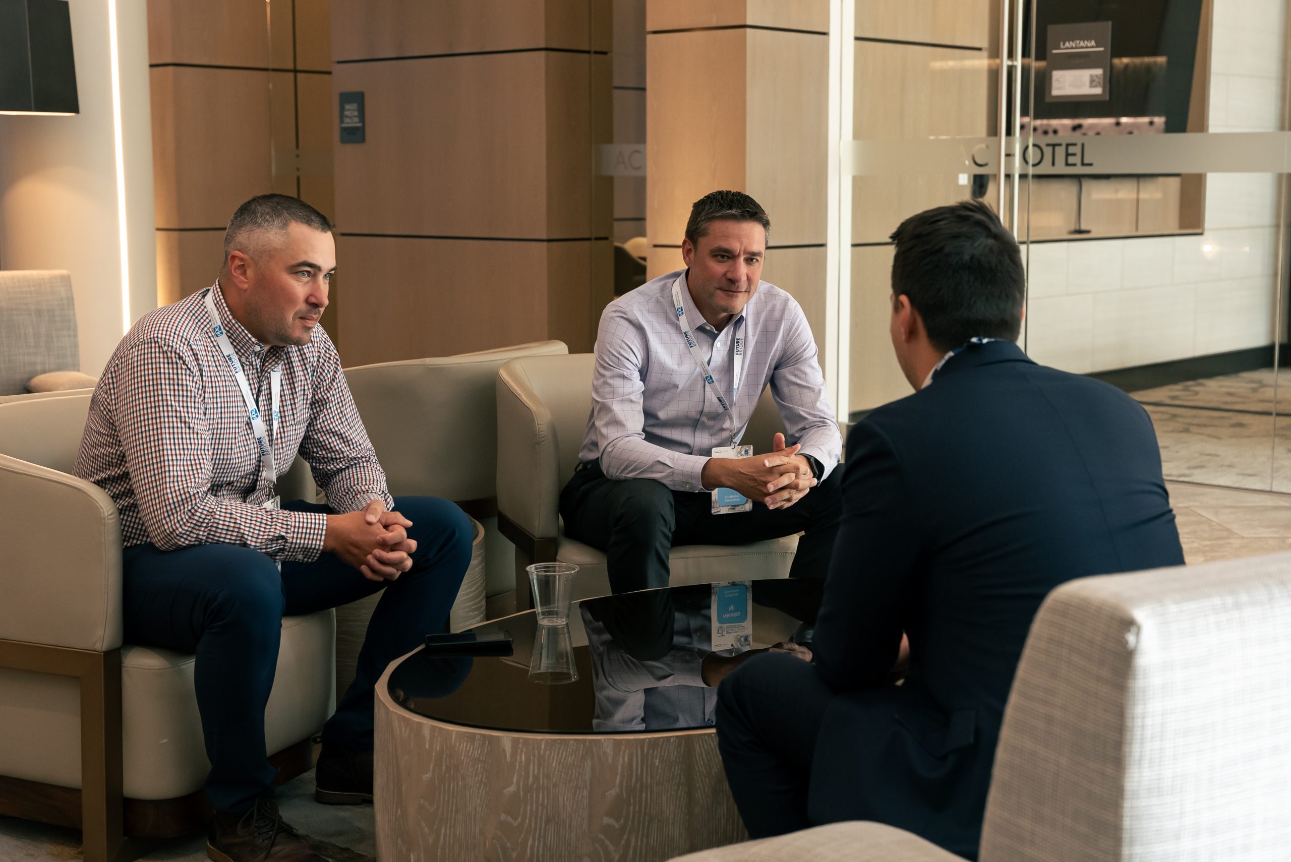
The agenda includes networking breaks featuring face-to-face meetings during coffee and ice-breaking sessions, designed to foster meaningful connections in a relaxed and informal setting.
-
Mobile App for Delegate ConnectionsFind, message and arrange meetings before and during the summit
-
Up to 6 Hours of Networking BreaksStructured time across the agenda, dedicated to conversation
-
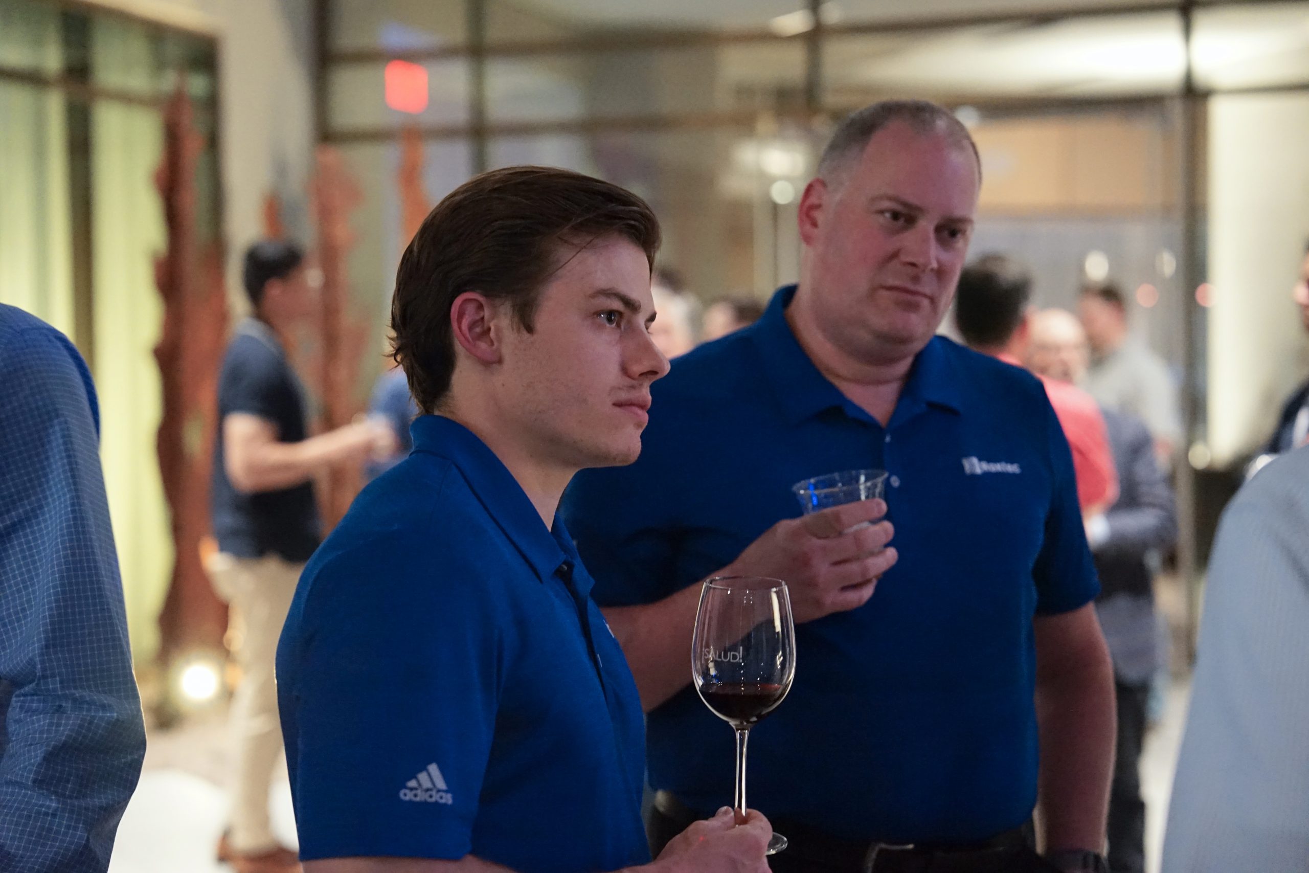
Drinks ReceptionAn informal close to day one, with the room already warmed up
-
Face-to-Face MeetingsCoffee and ice-breaking sessions built for focused discussion
-
Facilitated Peer-to-Peer NetworkingIntroductions between peers working the same problems on different sites
-
Post-Event CommunicationConnections continue after the summit closes, not just during it
Who should attend
Every function responsible for designing, building and operating Asia-Pacific semiconductor facilities.
Previous series attendees
& Sponsors
Fabs, foundries, IDMs, EPCs, cleanroom and MEP specialists, utilities providers and digital construction platforms from across the previous series.
The 7th Semiconductor Fab Design, Engineering & Construction Summit Asia Pacific is an excellent platform to elevate your company's profile within the semiconductor manufacturing and facility infrastructure sector, showcase your solutions, and enable high-value networking with the decision-makers delivering fab and advanced packaging projects across the region.
Direct C-suite access
Connect with senior executives, facilities leaders and decision-makers driving major fab and packaging projects across Asia-Pacific.
Brand visibility & credibility
Position your brand alongside industry leaders, presented to a targeted, pre-qualified audience of fab professionals.
Market intelligence
Gain real-time insight into APAC trends, procurement priorities and project pipelines from the executives leading them.
Premium experience
Our focused format guarantees every partner dedicated attention, prime visibility and full support to maximise ROI.
Thought leadership
Align your organisation with the people shaping the future of Asia-Pacific semiconductor manufacturing.
Technology showcase
Present your innovations to an audience actively sourcing solutions for fab construction and facility operations.
andrea@future-bridge.eu
vaishnavi@future-bridge.events
What past attendees say
Hear from attendees of previous Future Bridge semiconductor summits as they share their experiences, insights and key takeaways — from networking opportunities to thought-provoking sessions led by industry experts.
What delegates take back to site
-
“
Great networking, speaking, and learning opportunity. Most in attendance were very valuable contacts to make, and I learned a lot about the industry and region.
-
“
Great event. A lot of insights in the industry trends related to fab design & construction.
-
“
Thank you again for putting on such a great event. We really enjoyed attending, and the ASU factory tour was a highlight for me — very well done.
-
“
It was really good, all the presentations were really interesting and it was an excellent idea to include the visit to the ASU Factory.
-
“
Excellent event to connect with the semicon manufacturers.
-
“
It was a truly enriching experience to be part of this conclave, gaining valuable insights from industry leaders, innovators, and change-makers. The opportunity to learn from their experiences and perspectives was both inspiring and impactful.
-
“
Very useful to hear about latest developments and networking with people in our industry.
Gain cutting-edge knowledge and connect with industry innovators
Build Valuable Connections
Meet the peers, contractors and suppliers actively delivering fab and packaging projects across Asia-Pacific.
Stay Ahead Of Industry Trends
Track where APAC capacity, grid, water and cleanroom requirements are heading through 2030.
Interactive Learning With Experts
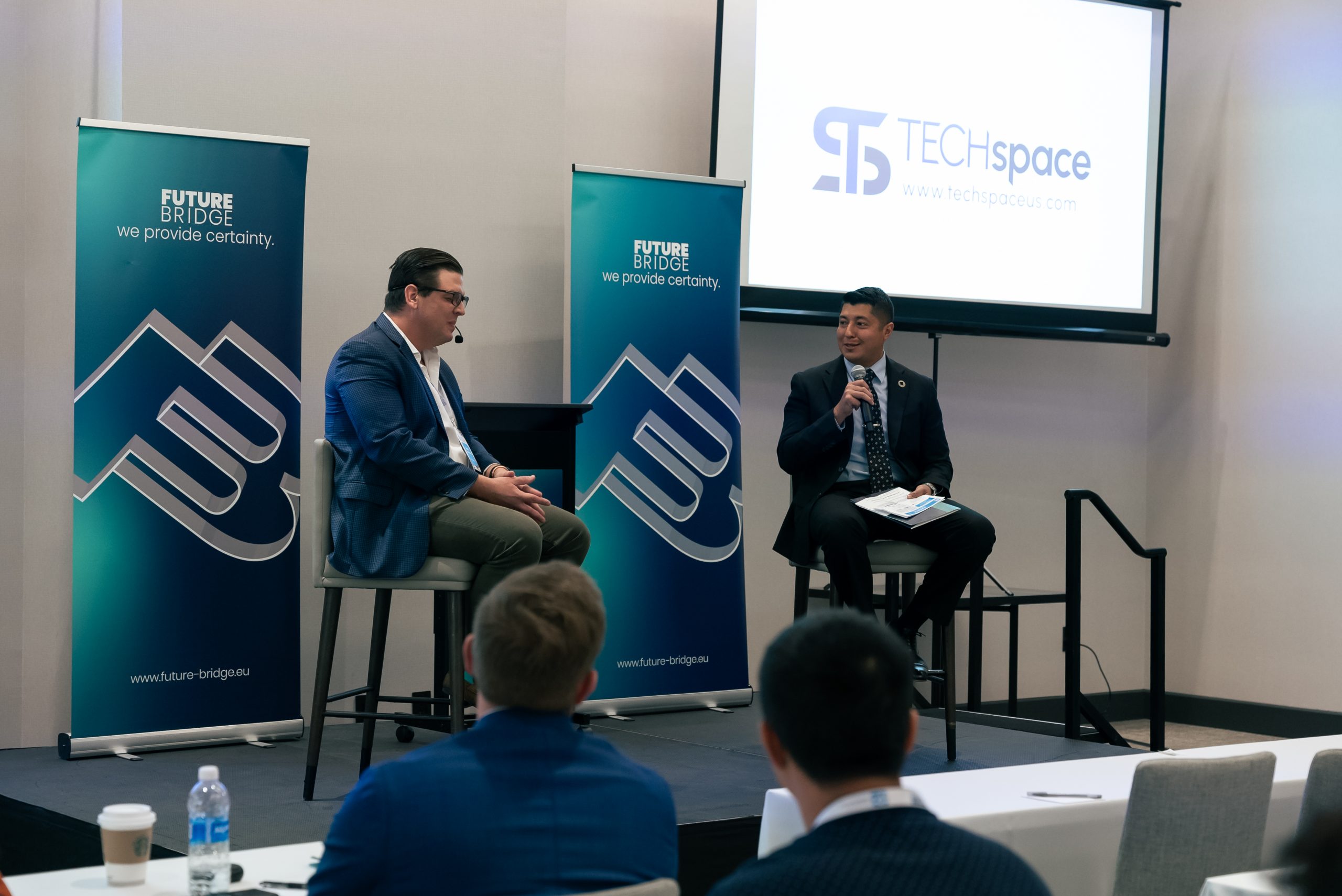
Panel discussions and case studies from senior facilities, utilities and construction leaders.
Exclusive Networking Opportunities
Face-to-face meetings, a drinks reception and continued connections after the event.
Get the full agenda
Access the complete programme — topics, format details, sponsorship packages and registration information for the 7th Semiconductor Fab Design, Engineering & Construction Summit Asia Pacific.
Choose your delegate category
All delegate passes include the full two-day programme, documentation and networking. Discounted prices apply until 6 August 2026.
Delegate
End-User
Applicable for: Semiconductor Manufacturing, Government Bodies, Semiconductor Associations, Universities and Research Facilities
Standard price 2 299 USD
399 USD
Discounted price until 6 August 2026
- 1 Delegate399 USD
- 2 Delegates599 USD
- 3 Delegates799 USD
- 2-Day Conference Pass
- Documentation Package
- Panel Discussions
- Refreshment Breaks And Lunches
- Drinks Reception
- Face To Face Networking
- Digital Certificate Of Attendance
Delegate
Solution Provider
Applicable for: Fab/facility design & engineering, Construction, Automation, HVAC & environmental control, Contamination & cleanroom solutions, Humidity control & filtration, Monitoring systems, Digital twin technology, Construction materials & equipment, Energy & storage solutions
Standard price 3 299 USD
1 399 USD
Discounted price until 6 August 2026
- 2-Day Conference Pass
- Documentation Package
- Panel Discussions
- Refreshment Breaks And Lunches
- Drinks Reception
- Face To Face Networking
- Digital Certificate Of Attendance
Delegate
Construction & Engineering
Applicable for: General contractors, EPC firms, MEP contractors, structural engineers, project management consultancies
Standard price 2 499 USD
1 199 USD
Discounted price until 6 August 2026
- 2-Day Conference Pass
- Documentation Package
- Panel Discussions
- Refreshment Breaks And Lunches
- Drinks Reception
- Face To Face Networking
- Digital Certificate Of Attendance
Exhibition Partner
Standard price 11 900 USD
7 900 USD
Discounted price until 6 August 2026
- Exhibition stand space
- 2 delegate passes
- Logo and company text in all conference materials
- Conference documentation package
Presenting Partner
Standard price 11 900 USD
8 900 USD
Discounted price until 6 August 2026
- Speaker slot
- 1 speaker attendee pass
- Logo and company text in all conference materials
- Conference documentation package
See the summit in action
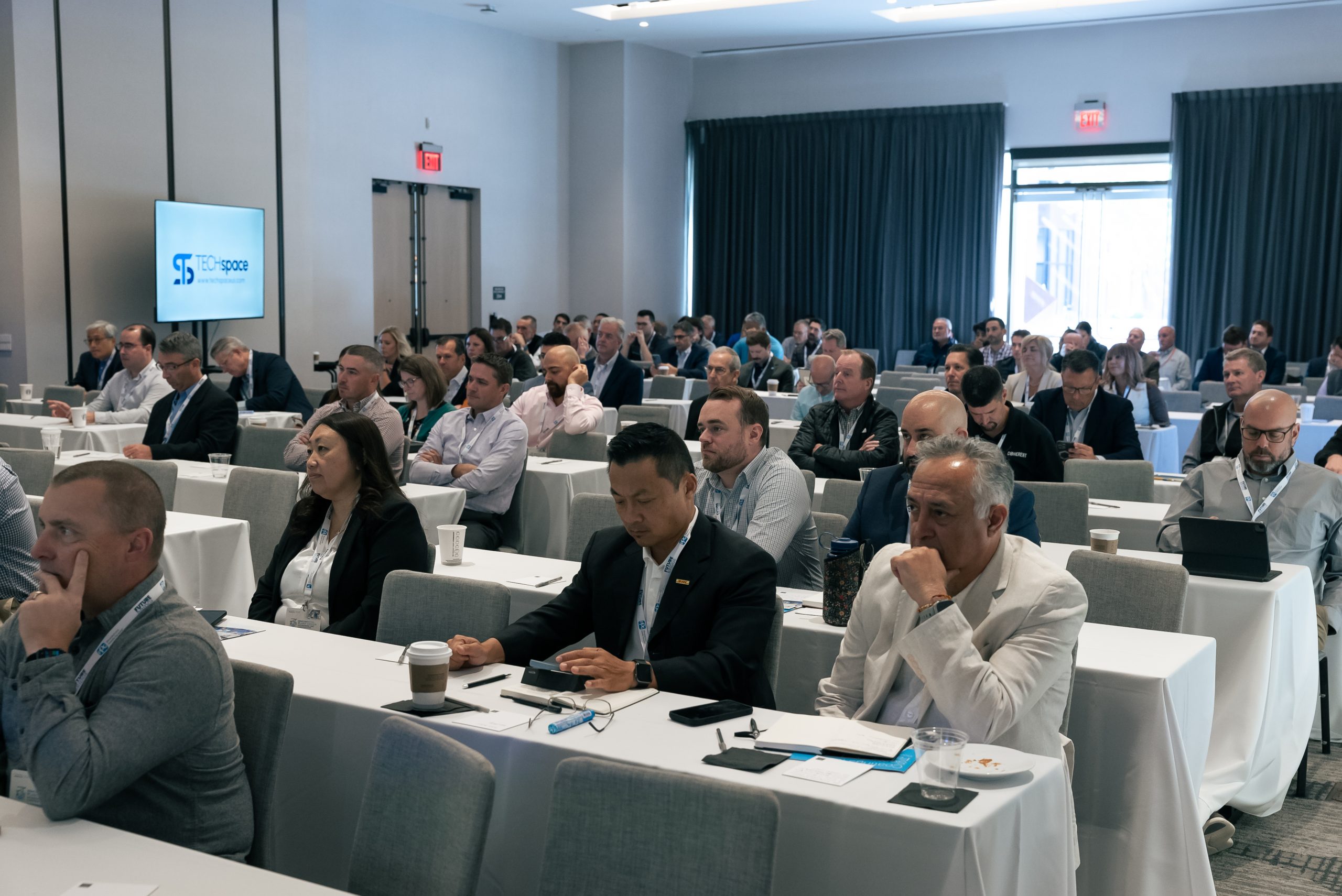
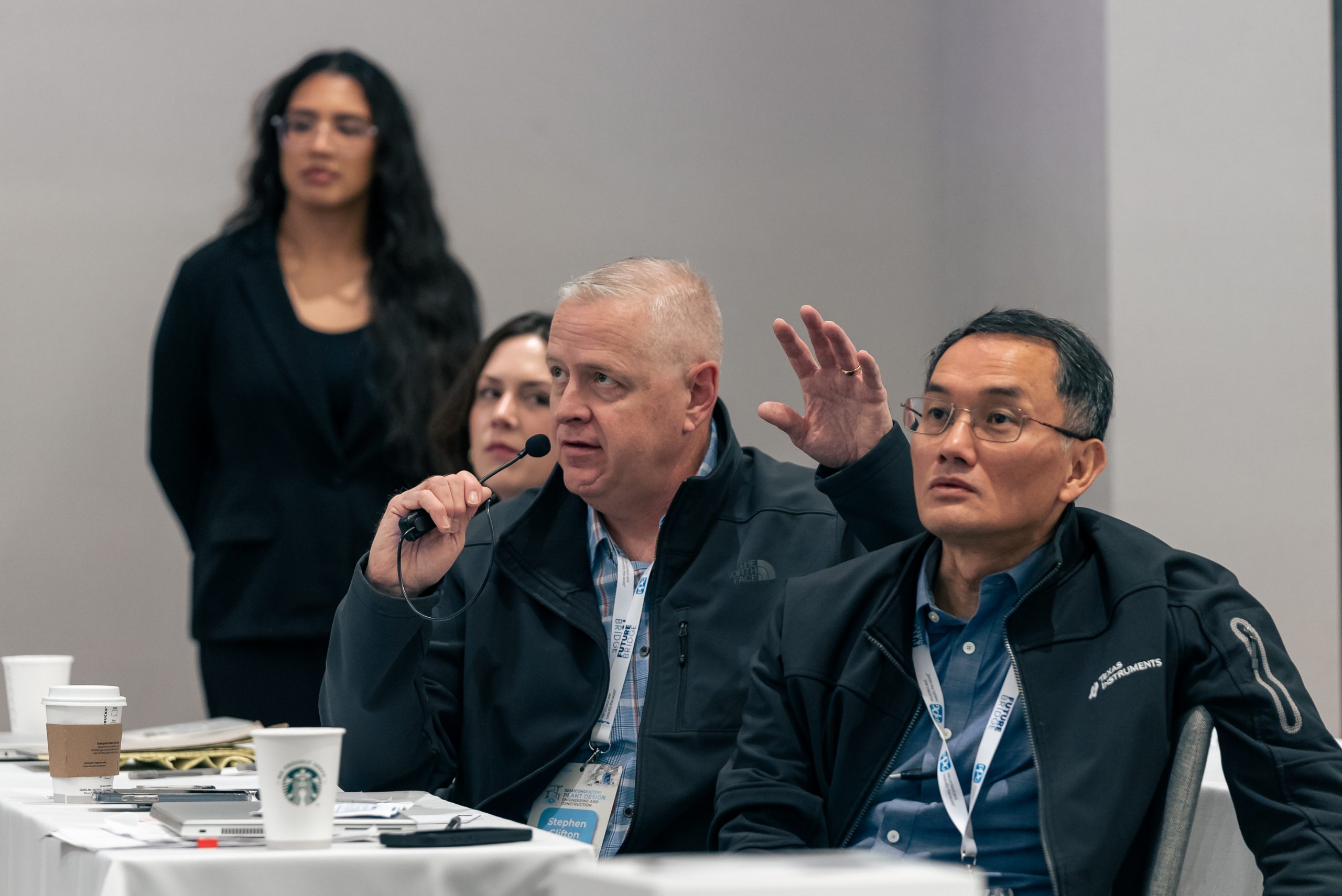
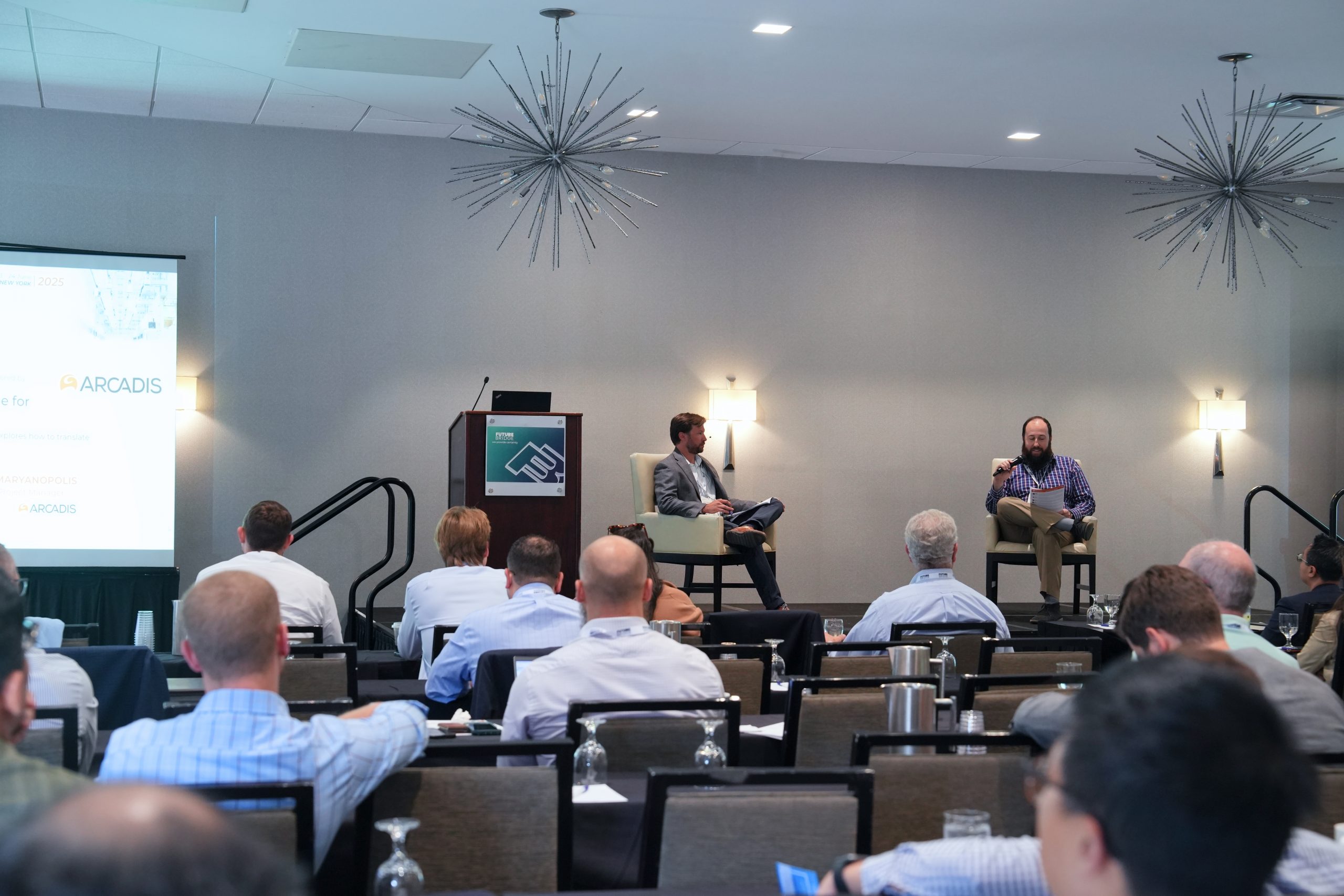
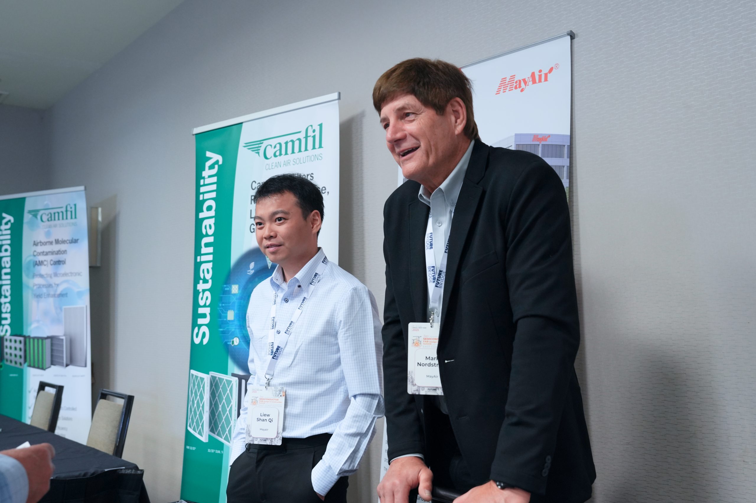
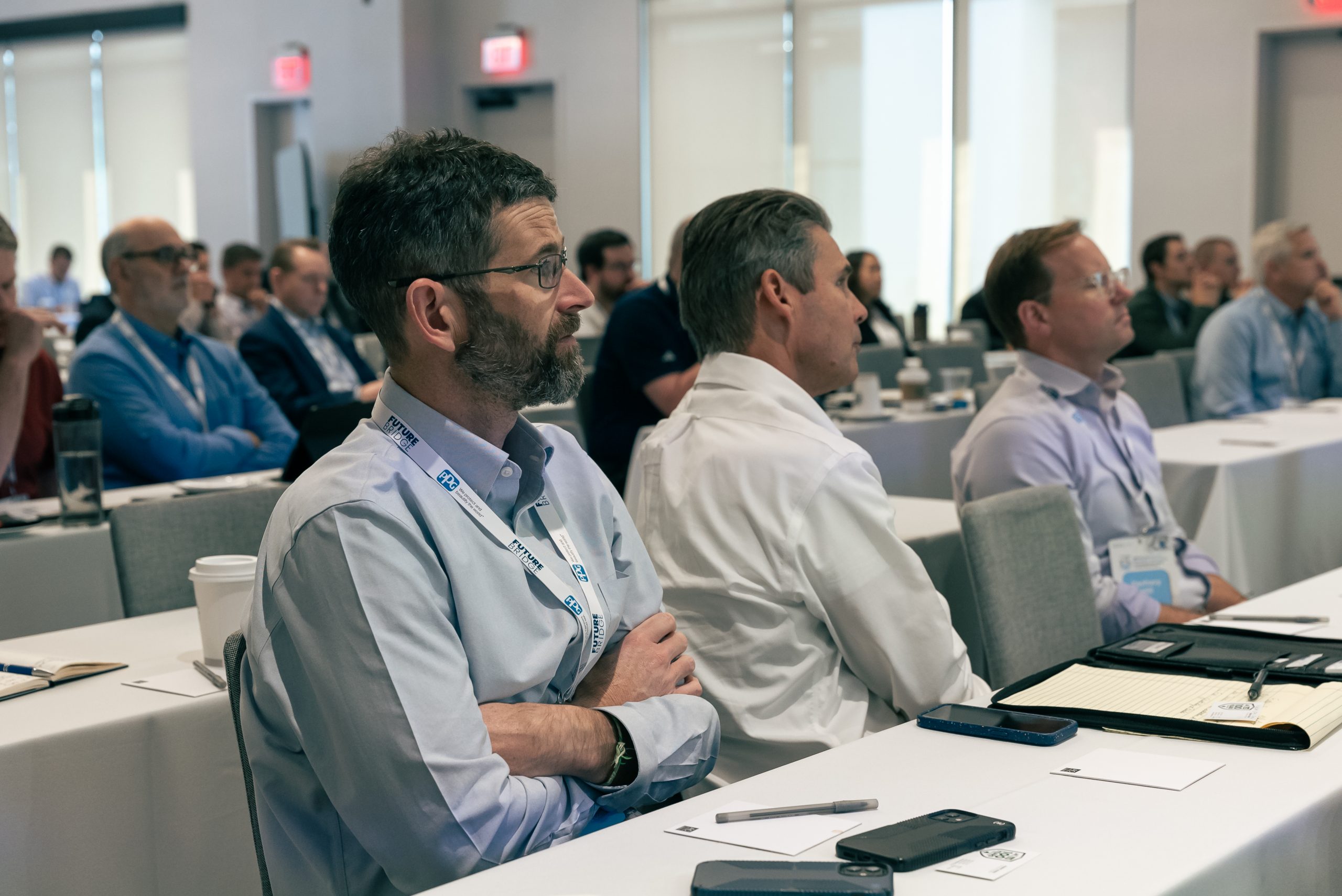
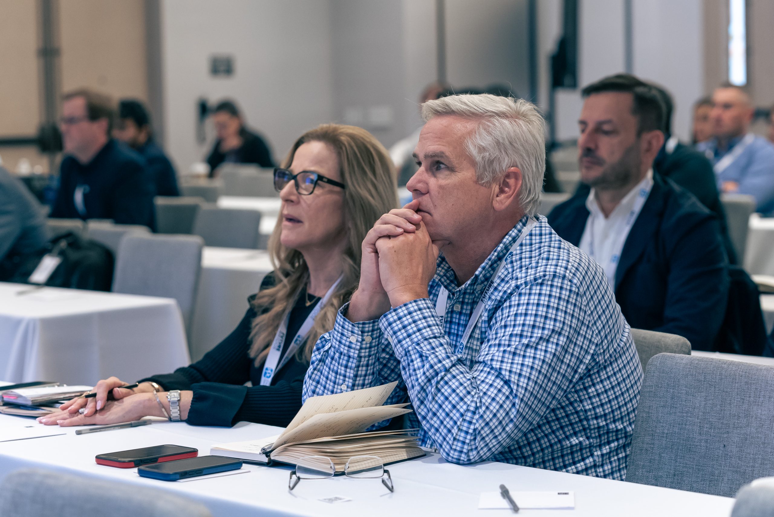
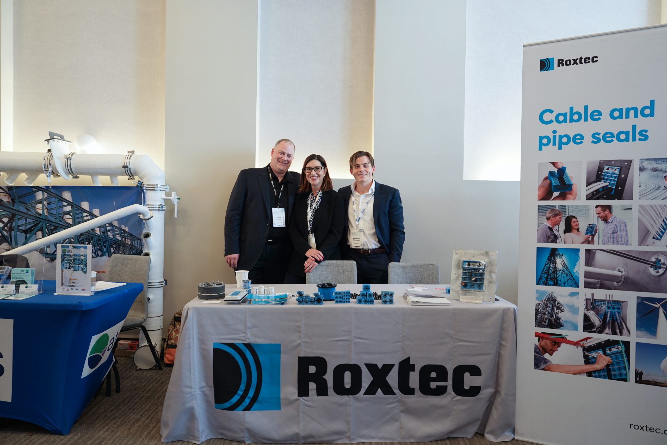
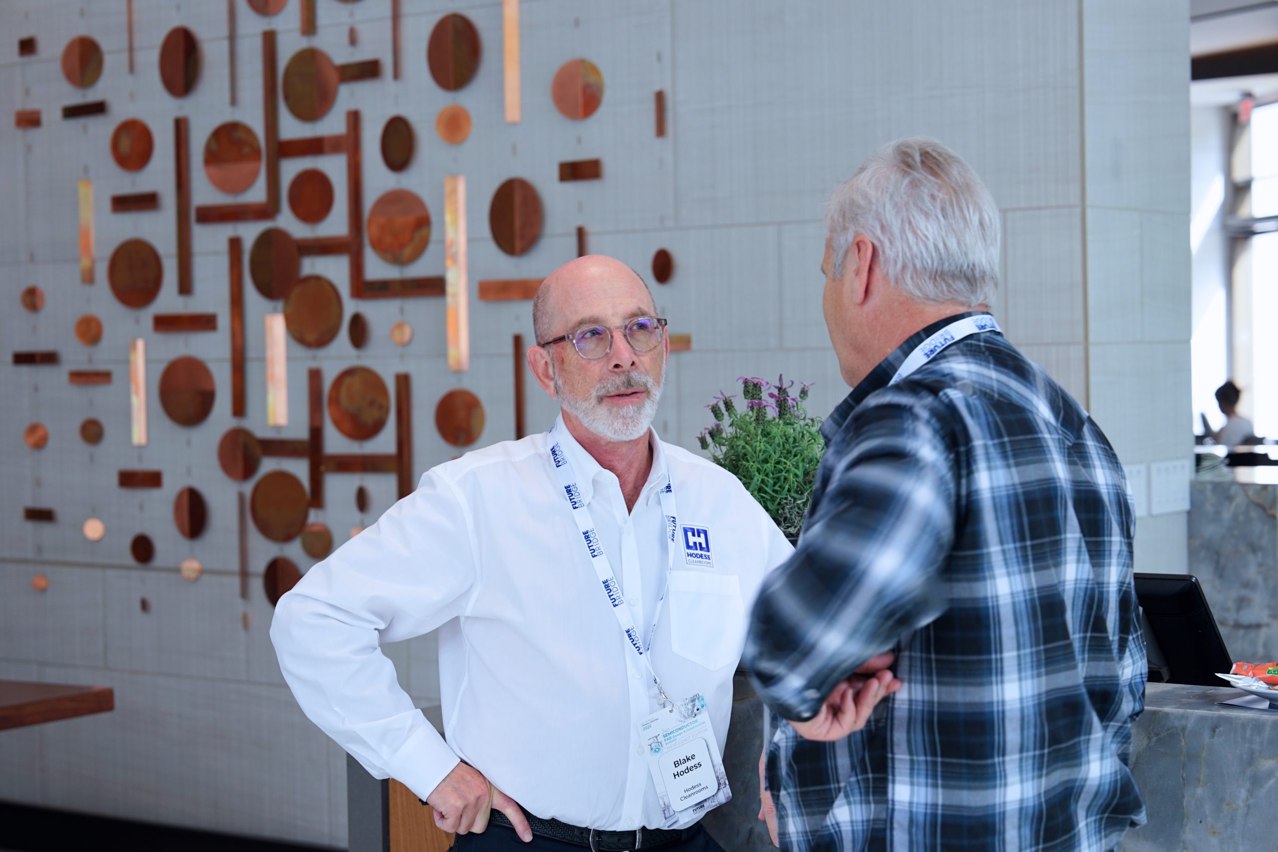
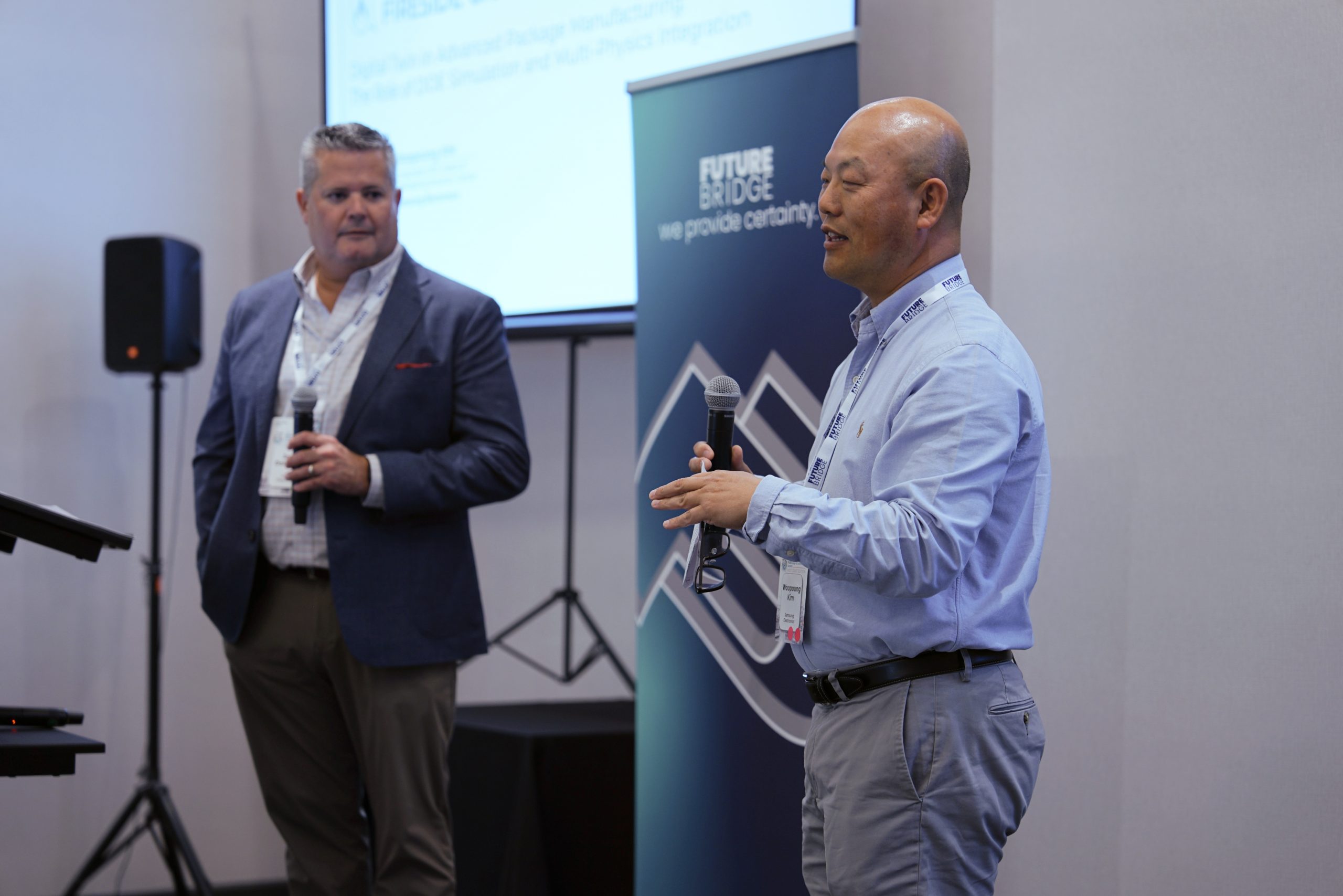
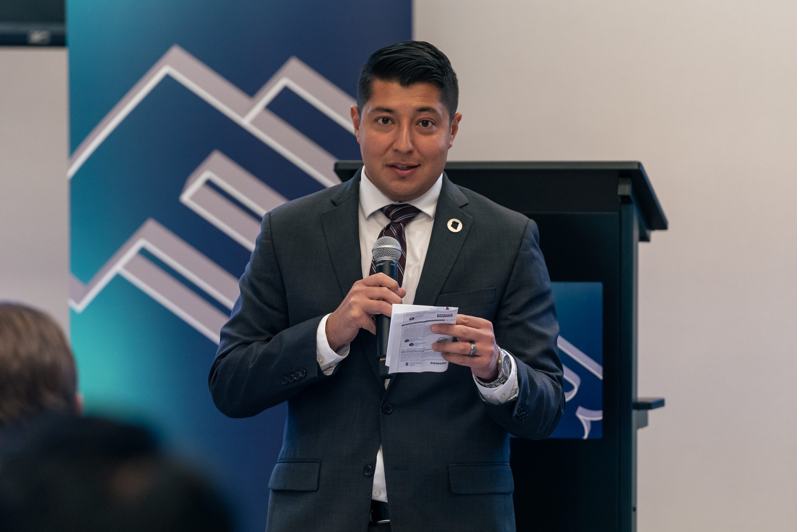
A look inside the Future Bridge semiconductor fab series — sessions, exhibition floor and the conversations between them.
Media Gallery
A look across the summit — sessions, the exhibition floor, networking and the people delivering Asia-Pacific fabs.

Privacy Overview
| Cookie | Duration | Description |
|---|---|---|
| cookielawinfo-checkbox-analytics | 11 months | This cookie is set by GDPR Cookie Consent plugin. The cookie is used to store the user consent for the cookies in the category "Analytics". |
| cookielawinfo-checkbox-functional | 11 months | The cookie is set by GDPR cookie consent to record the user consent for the cookies in the category "Functional". |
| cookielawinfo-checkbox-necessary | 11 months | This cookie is set by GDPR Cookie Consent plugin. The cookies is used to store the user consent for the cookies in the category "Necessary". |
| cookielawinfo-checkbox-others | 11 months | This cookie is set by GDPR Cookie Consent plugin. The cookie is used to store the user consent for the cookies in the category "Other. |
| cookielawinfo-checkbox-performance | 11 months | This cookie is set by GDPR Cookie Consent plugin. The cookie is used to store the user consent for the cookies in the category "Performance". |
| viewed_cookie_policy | 11 months | The cookie is set by the GDPR Cookie Consent plugin and is used to store whether or not user has consented to the use of cookies. It does not store any personal data. |