
The 6th Asia Pacific Semiconductor FAB Design Engineering & Construction Summit brought together professionals responsible for designing, engineering, constructing, and expanding semiconductor fabrication facilities across the Asia-Pacific region. Over two days in Singapore, the summit focused on facilities, utilities, capital project delivery, and infrastructure that support semiconductor manufacturing. Moreover, the programme featured keynote presentations, technical sessions, sponsor presentations, and panel discussions that explored practical engineering solutions, sustainability, digital technologies, water systems, and project execution for semiconductor fabs.
Day One highlights from the 6th Asia Pacific Semiconductor FAB Design Engineering & Construction Summit
Day One covered technical topics that support semiconductor facility development from planning through operations. First, speakers discussed decarbonisation and semiconductor water systems. Next, they explored reliable power, Digital Twin technology, and manufacturing challenges. Afterwards, the programme shifted to helium recovery, water treatment, and project delivery before concluding with networking opportunities for delegates.
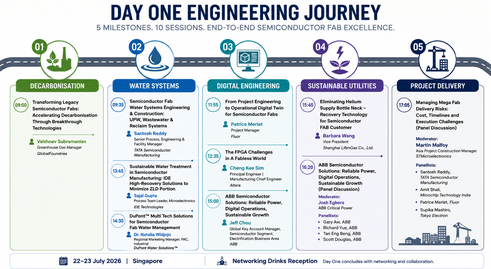
Transforming Legacy Semiconductor Fabs: Accelerating Decarbonisation Through Breakthrough Technologies
Speaker:
Vaishnav Subramanian
Greenhouse Gas Manager, GlobalFoundries
Vaishnav Subramanian opened the technical programme with the keynote address. First, he discussed breakthrough decarbonisation technologies that reduce semiconductor manufacturing emissions. Next, he explained strategies for eliminating most Scope 1 emissions within the next decade. Furthermore, he covered methods for transforming legacy fabs while maintaining operational efficiency and production continuity. Finally, the session addressed environmental strategy, long-term fab modernisation, expansion planning, key challenges, lessons learned, & opportunities for sustainable semiconductor manufacturing at scale.
Semiconductor Fab Water Systems Engineering & Construction: UPW, Wastewater & Reclaim Systems
Speaker:
Santosh Reddy
Senior Process, Engineering & Facility Manager, TATA Semiconductor Manufacturing
Next, Santosh Reddy presented a session on semiconductor fab water systems engineering and construction. He introduced Ultra Pure Water (UPW), wastewater treatment plants, and reclaim systems. Moreover, he explained the system overview and the Basis of Design (BOD). In addition, he discussed engineering considerations for UPW, wastewater, and reclaim systems. Additionally, he examined construction challenges that engineering teams encounter while developing semiconductor water infrastructure for fabrication facilities.
ABB Semiconductor Solutions: Reliable Power, Digital Operations, Sustainable Growth
Speaker:
Jeff Chou
Global Key Account Manager, Semiconductor Segment, Electrification Business Area, ABB
Jeff Chou delivered ABB’s Gold Sponsor presentation on reliable power and digital operations. First, he explained how uninterrupted power supports semiconductor manufacturing. Next, he discussed smart asset management for fab operations. Additionally, he covered sustainable manufacturing practices that support operational performance. Furthermore, throughout the presentation, the session focused on optimising fab operations. This is through reliable electrical infrastructure, digital operations, and sustainable manufacturing solutions developed by ABB.
ABB Semiconductor Solutions: Reliable Power, Digital Operations, Sustainable Growth (Panel Discussion)
Moderator: Josh Egbers, ABB Critical Power
Panellists: Gary Aw, Richard Yue, Tan Eng Beng and Scott Douglas, ABB
Later, ABB continued the discussion through a panel session. Josh Egbers moderated the discussion, while Gary Aw, Richard Yue, Tan Eng Beng, and Scott Douglas joined as panellists. Together, they discussed reliable power, digital operations, and sustainable manufacturing for semiconductor facilities. Furthermore, the panel continued the conversation around uninterrupted power, smart asset management, and sustainable manufacturing that formed the focus of ABB’s earlier presentation.
From Project Engineering to Operational Digital Twin for Semiconductor Fabs
Speaker:
Patrice Merlet
Project Manager, Fluor
Patrice Merlet presented a session on Digital Twin implementation for semiconductor manufacturing facilities. First, he discussed leveraging Digital Twin technology in advanced semiconductor fabs. Next, he explained BIM, structured asset information, and IIoT for lifecycle integration. Moreover, he covered Digital Twin use cases during project execution. Finally, the presentation examined operational efficiency, predictive maintenance, and a practical roadmap for implementing Digital Twin technology across semiconductor facilities.
The FPGA Challenges in A Fabless World
Speaker:
Cheng Kee Sim
Principal Engineer | Manufacturing Chief Engineer, Altera
Cheng Kee Sim discussed FPGA manufacturing within today’s semiconductor industry. First, he explained the role FPGA technology plays in semiconductor manufacturing. Next, he outlined challenges that are unique to FPGAs compared with ASICs. Finally, he discussed how FPGA companies overcome those challenges. The session focused on technical and manufacturing considerations associated with FPGA development in a fabless environment
Eliminating Helium Supply Bottleneck – Recovery Technology for Semiconductor FAB Customer
Speaker:
Barbara Wang
Vice President, Shanghai LifenGas Co., Ltd.
Barbara Wang presented Shanghai LifenGas’ Bronze Sponsor session on helium recovery technology for semiconductor fabs. First, she explained that the recovery and reuse of more than 80% of helium is possible, as documented in case studies. Next, she discussed achieving helium purity of up to 99.999% using a reliable and mature design for fab operations. Finally, she explained how helium recovery technology can increase supply reliability while delivering significant cost savings for semiconductor manufacturers.
DuPont™ Multi Tech Solutions for Semiconductor Fab Water Management
Speaker:
Dr. Natalia Widjojo
Regional Marketing Manager, PAC, Industrial, DuPont Water Solutions™
Next, Dr. Natalia Widjojo presented DuPont Water Solutions’ Bronze Sponsor session on semiconductor fab water management. She discussed delivering high-quality Ultra Pure Water (UPW) for semiconductor manufacturing facilities. Moreover, she explained approaches that enable minimal liquid discharge through 3R wastewater strategies. The presentation focused on recycle, reuse, and reduce practices that support semiconductor water management while addressing wastewater generated during fabrication processes.
Sustainable Water Treatment in Semiconductor Manufacturing: IDE High-Recovery Solutions to Minimize ZLD Portion
Speaker:
Sajal Gupta
Process Team Leader, Microelectronics, IDE Technologies
Afterwards, Sajal Gupta delivered IDE Technologies’ Presenting Partner session on sustainable water treatment for semiconductor manufacturing. First, he reviewed the current water landscape in the global semiconductor sector. Next, he introduced IDE’s high-recovery technologies, including PFRO and Desalter solutions. Furthermore, he discussed the economic implications of adopting high-recovery technologies. Finally, he explained the sustainability outcomes of these solutions and their role in minimising the Zero Liquid Discharge (ZLD) portion.
Managing Mega Fab Delivery Risks: Cost, Timelines and Execution Challenges
Moderator:
Martin Malfoy
Asia Project Construction Manager, STMicroelectronics
Panellists:
Santosh Reddy – TATA Semiconductor Manufacturing
Amit Shali – Microchip Technology India
Patrice Merlet – Fluor
Supika Mashiro – Tokyo Electron
Finally, the closing panel discussion examined key challenges in semiconductor project delivery. First, the panellists discussed supply chain and contractor risks. Next, they compared EPC, EPCM, and alliance delivery models. They also explored methods for managing cost escalation and schedule pressure. Finally, the panel shared lessons learned from recent semiconductor fab projects before the Chairman concluded Day One and delegates moved to the networking drinks reception.
Day Two highlights from the 6th Asia Pacific Semiconductor FAB Design Engineering & Construction Summit
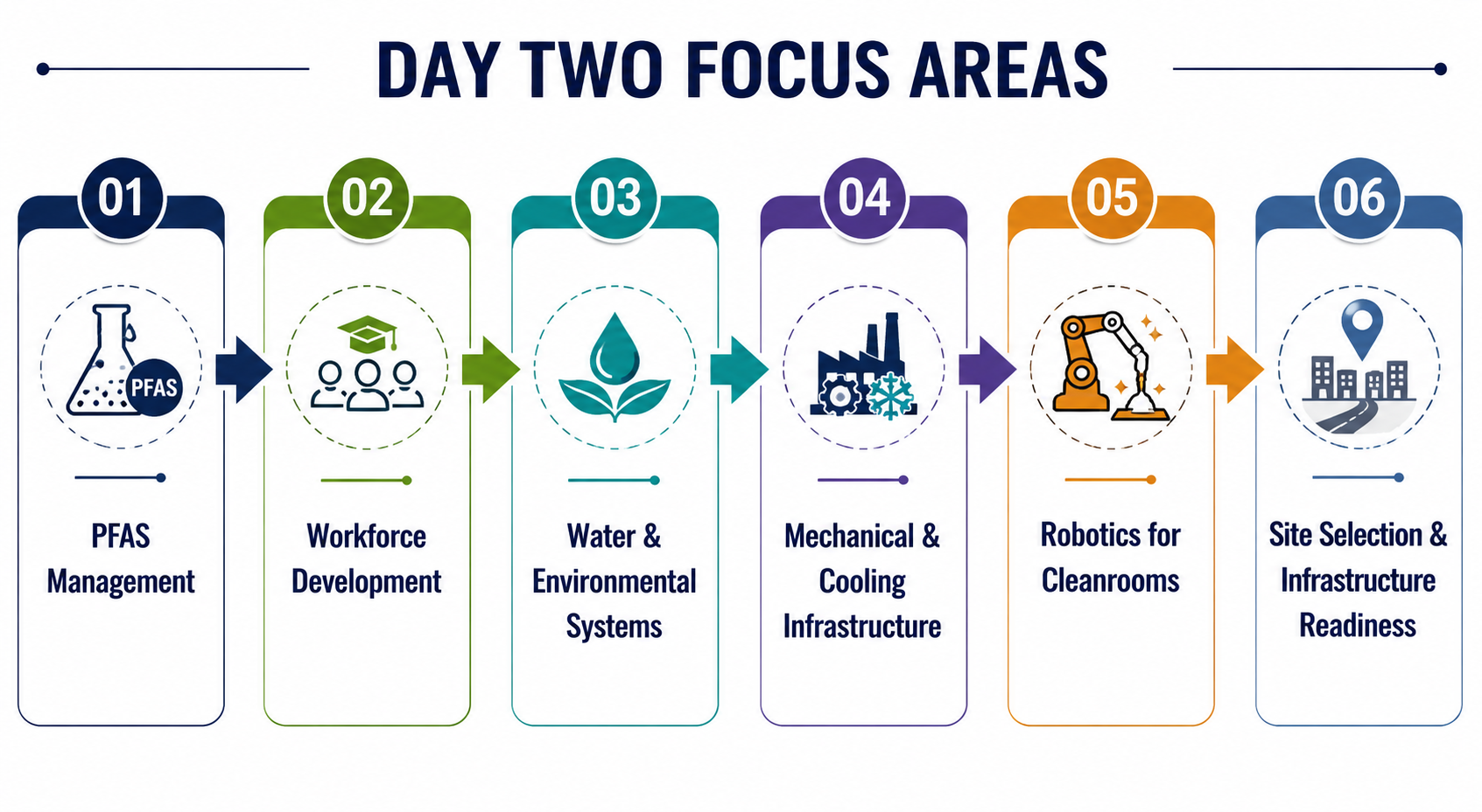
The second day of the 6th Asia Pacific Semiconductor FAB Design Engineering & Construction Summit focused on environmental management, workforce capability, water systems, mechanical infrastructure, robotics, and site selection. First, speakers discussed sustainability and regulatory topics affecting semiconductor manufacturing. Next, technical experts shared practical approaches for improving water, cooling, and cleanroom operations. Finally, the programme concluded with a brainstorming session on infrastructure readiness across the Asia-Pacific region before the conference closed.
Industry-Wide Action on PFAS: Collaboration, Standards, and the Road Ahead — A SEMI Member Perspective —
Speaker:
Supika Mashiro
Advisor, Tokyo Electron
Supika Mashiro opened Day Two with a session on PFAS management in semiconductor manufacturing. First, she discussed PFAS concerns from sustainability and regulatory perspectives. Next, she provided an overview of PFAS use in semiconductor manufacturing. Moreover, she explained the industry’s PFAS management strategy and current actions. Finally, she examined PFAS risks and opportunities for a SEMI member equipment supplier while encouraging collaboration across the semiconductor industry.
Workforce Development, Training & Capability Building in New Markets
Speaker:
Amit Shali
Manager, Software and Academic Partnerships (APAC), Microchip Technology India
Next, Amit Shali discussed workforce development across emerging semiconductor markets. First, he explained the APAC workforce development opportunity. Afterwards, he explored collaboration between industry, academia, and government. In addition, he discussed STEM engagement, academic partnerships, reskilling, and upskilling initiatives. Finally, he explained how training programmes support capability building, bridge skill gaps, and strengthen long-term competitiveness within the semiconductor industry.
Advancing Sustainable Water and Environmental Systems for Semiconductor Facilities
Speaker:
Steven Lam
Head of Technology, Gradiant
Steven Lam delivered Gradiant’s Presenting Partner session on water and environmental systems. First, he discussed implementing high-efficiency wastewater treatment technologies. Next, he explained strategies for optimising water reuse. Furthermore, he covered system design for regulatory compliance. Finally, he showed how these approaches support long-term sustainability goals for semiconductor facilities while improving water management throughout manufacturing operations.
Optimizing Mechanical Systems and Cooling Infrastructure for Fab Efficiency
Speaker:
Prithvi Chandrashekar
Business Line Manager, Oil Free Air Division, Atlas Copco (SEA) Pte Ltd
Prithvi Chandrashekar presented Atlas Copco’s session on mechanical systems and cooling infrastructure. First, he discussed improving energy efficiency in compressed air generation. Next, he explained savings through HOC technology. Moreover, he introduced Triple Class Zero air quality solutions. Finally, he covered hot water generation during compressor operation with 80% savings and explained how adiabatic coolers help reduce plant water consumption.
RADAC: Robot-Aided Cleaning and Sanitisation for ISO Class Cleanrooms
Speaker:
Dr. Veerajagadheswar Prabakaran
Research Fellow, Singapore University of Technology and Design (SUTD)
Dr. Veerajagadheswar Prabakaran introduced RADAC, a collaboration between SUTD and A*STAR ARTC. First, he presented an autonomous robot that cleans and sanitises cleanroom floors without human entry. Next, he explained the cleaning payload design and automatic mop-pad exchange through a docking station. Finally, he discussed adaptable coverage planning for cluttered fab layouts and opportunities for future pilot partnerships.
Engineering Site Selection and Industrial Infrastructure Readiness Across APAC
Session: Brainstorming Session
The conference concluded with a brainstorming session on engineering site selection across the Asia-Pacific region. First, participants discussed evaluating power, water, and logistics infrastructure. Next, they explored permitting and regulatory requirements. Furthermore, the discussion covered coordination with industrial parks and government authorities. Finally, participants examined methods for assessing risks across different APAC markets before the conference concluded with the final networking lunch.
Sponsors and partners at the 6th Asia Pacific Semiconductor FAB Design Engineering & Construction Summit
The 6th Asia Pacific Semiconductor FAB Design Engineering & Construction Summit featured support from technology companies specialising in power systems, water treatment, industrial gases, and semiconductor infrastructure. Throughout the event, sponsors and partners contributed through technical presentations, case studies, and exhibition activities. The following organisations participated in different sponsorship categories.
ABB (Gold Sponsor)
ABB participated as the Gold Sponsor of the summit. The company is a global technology leader in electrical distribution and energy management. Furthermore, it operates in more than 100 countries with over 50,000 employees. Moreover, ABB works with customers and partners to support safe, smart, and sustainable electrification. Additionally, during the summit, the company also delivered presentations on reliable power, digital operations, and sustainable manufacturing for semiconductor facilities.
DuPont Water Solutions (Bronze Sponsor)
DuPont Water Solutions participated as a Bronze Sponsor. Moreover, the company provides ion exchange resins, reverse osmosis, nanofiltration, ultrafiltration, membrane aerated biofilm reactors (MABR), membrane bioreactors (MBR), and electrodeionisation technologies. Additionally, these solutions support industrial water, wastewater, water reuse, pharmaceuticals, industrial processes, power, and municipal applications. The company also aligns its work with the United Nations 2030 Sustainable Development Goals.
Shanghai LifenGas Co., Ltd. (Bronze Sponsor)
Shanghai LifenGas Co., Ltd. participated as a Bronze Sponsor. Founded in 2018, the company focuses on gas separation, purification equipment, energy-saving technologies, and environmental solutions. Furthermore, its products serve industries including semiconductors, photovoltaics, batteries, chemicals, glass, steel, and automotive manufacturing. The company also operates an ISO9001-certified manufacturing facility in Jiangsu Province and provides 24/7 after-sales support through multiple service centres in China.
IDE Technologies (Presenting Partner)
IDE Technologies participated as a Presenting Partner. The company provides wastewater treatment solutions for semiconductor manufacturing during wafer production and End of Pipe (EOP) stages. Moreover, its portfolio includes reuse, reclaim, and recycle systems that reduce wastewater discharge, lower raw water consumption, and support environmental protection. Moreover, the company also helps manufacturers meet water quality standards. This is while reducing carbon and water footprints through advanced wastewater management solutions.
Gradiant (Presenting Partner)
Gradiant participated as a Presenting Partner. The company provides advanced water and wastewater solutions for semiconductor manufacturing facilities. Furthermore, its portfolio includes Ultra Pure Water systems, DI water systems, wastewater treatment, water reuse, advanced brine concentration, and Zero Liquid Discharge technologies. Additionally, the company offers its AI-powered SmartOps™ platform to help optimise water recovery, utility performance, operating costs, and production continuity.
Atlas Copco (Presenting Partner)
Atlas Copco participated as a Presenting Partner. The company has operated in Singapore since 1979. It provides compressors, vacuum systems, generators, pumps, power tools, and assembly solutions for industrial applications. Additionally, the company focuses on helping businesses improve productivity and efficiency through a range of industrial technologies and engineering solutions.
BW Water (Exhibition Partner)
BW Water participated as the Exhibition Partner. The company provides water and wastewater solutions for municipal and industrial applications. Furthermore, it has developed more than 200 installations worldwide and employs around 300 people. Moreover, BW Water operates across nine global locations. Its headquarters are in Singapore, while its regional hubs in Florida and Stuttgart support operations across the Americas and EMEA.
Looking Ahead
The 6th Asia Pacific Semiconductor FAB Design Engineering & Construction Summit brought together semiconductor manufacturers, engineering experts, technology providers, and infrastructure specialists. This was to exchange practical knowledge on semiconductor facility development. Furthermore, throughout the two-day programme, delegates explored technical solutions, shared project experiences, and built new industry connections. So, if you want to stay updated on the latest developments in semiconductor fab design, engineering, construction, and utilities, consider attending future Summits to gain fresh insights and expand your professional network.