
Why Attend?
1
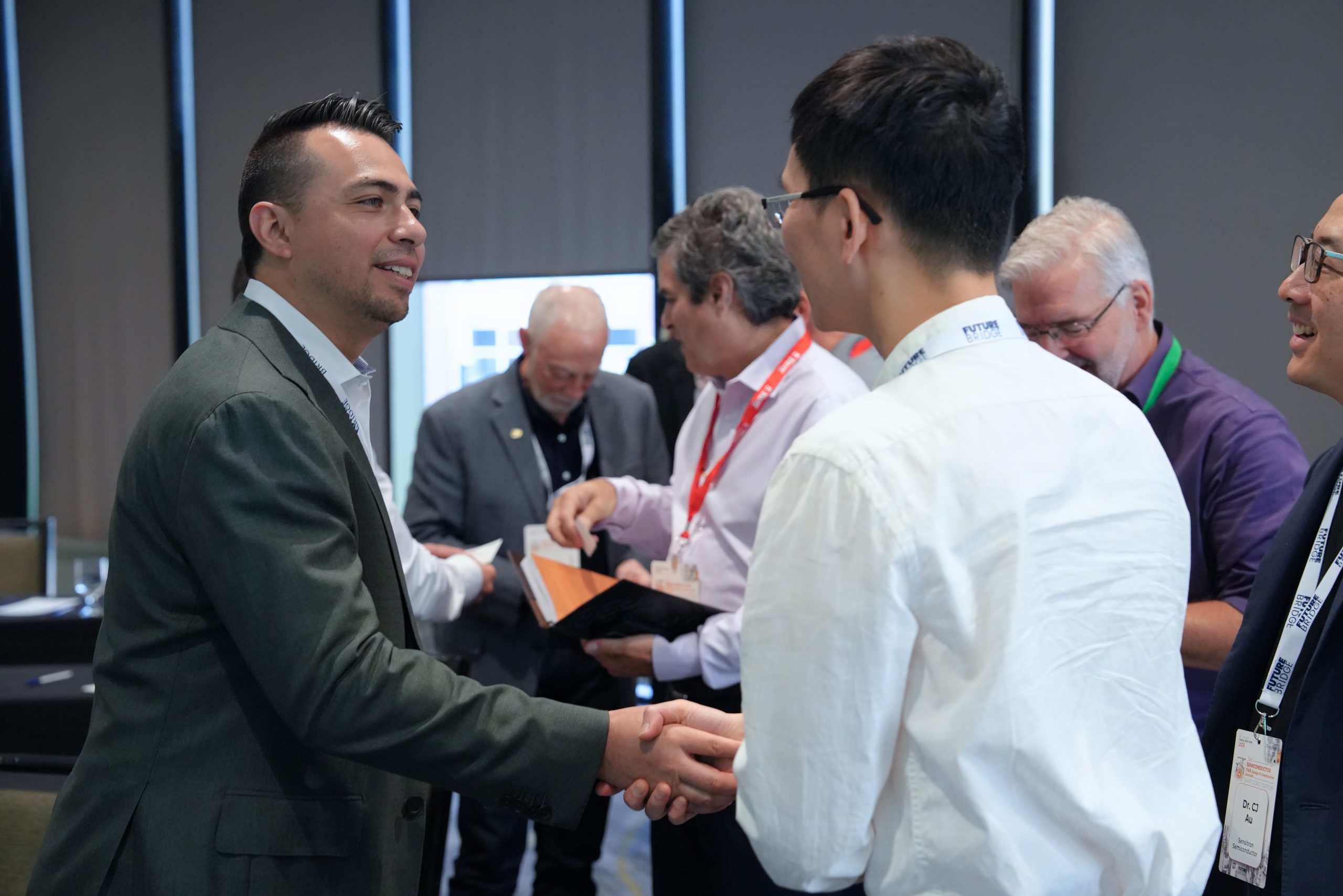
Build Valuable Connections
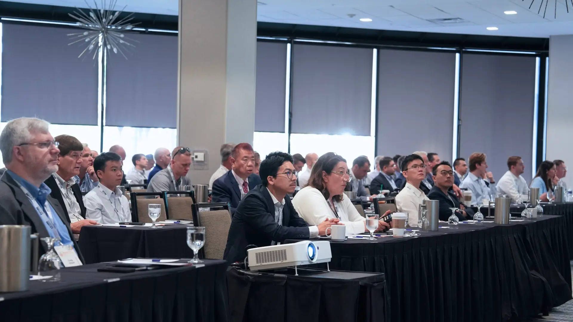
Network with 100+ senior facilities, utilities, construction and industrial park leaders from across Asia-Pacific
2
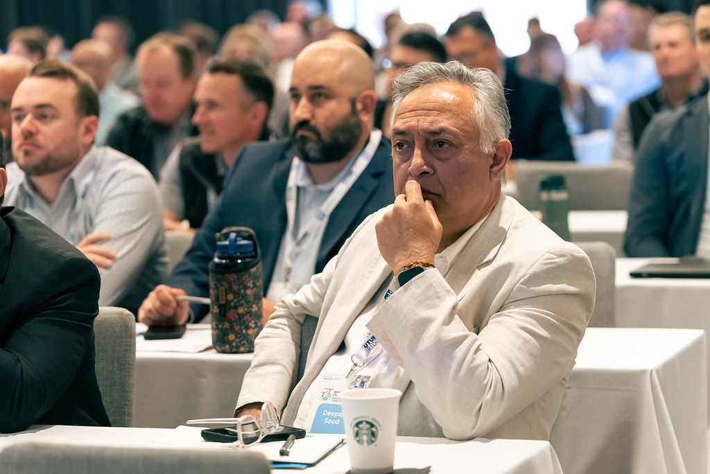
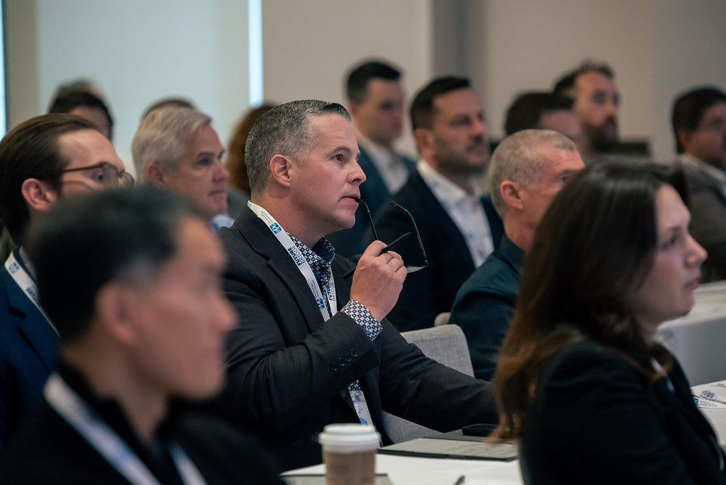
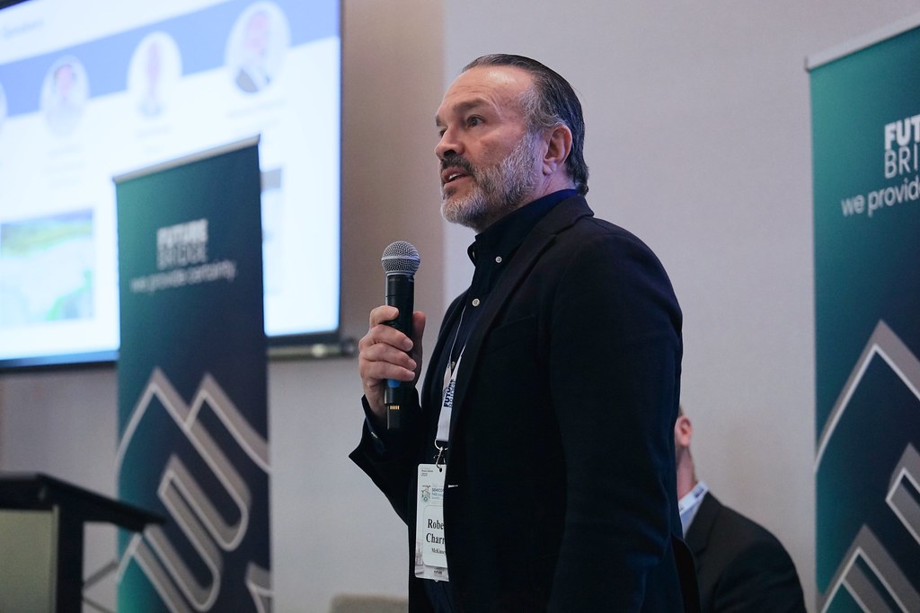
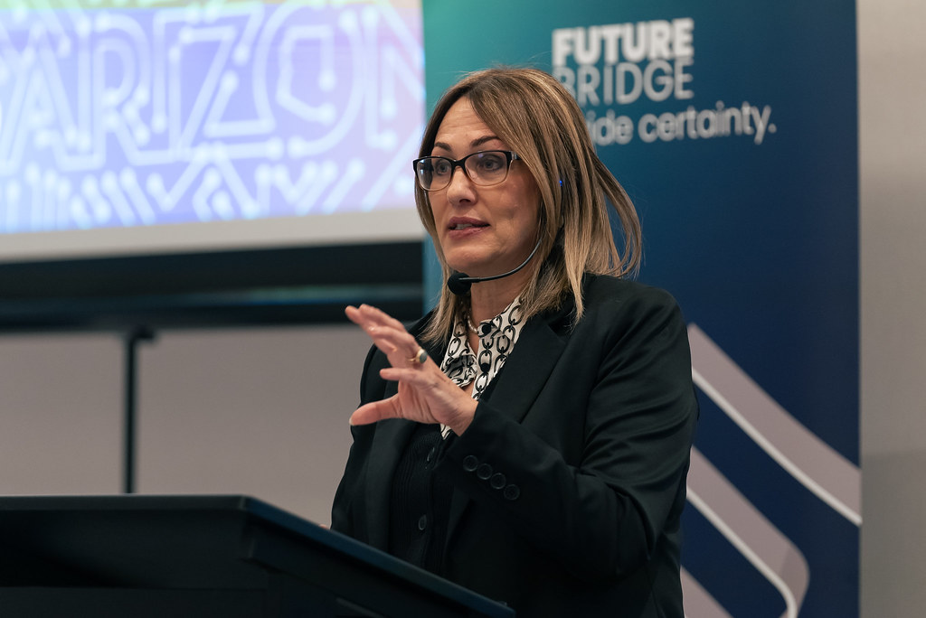
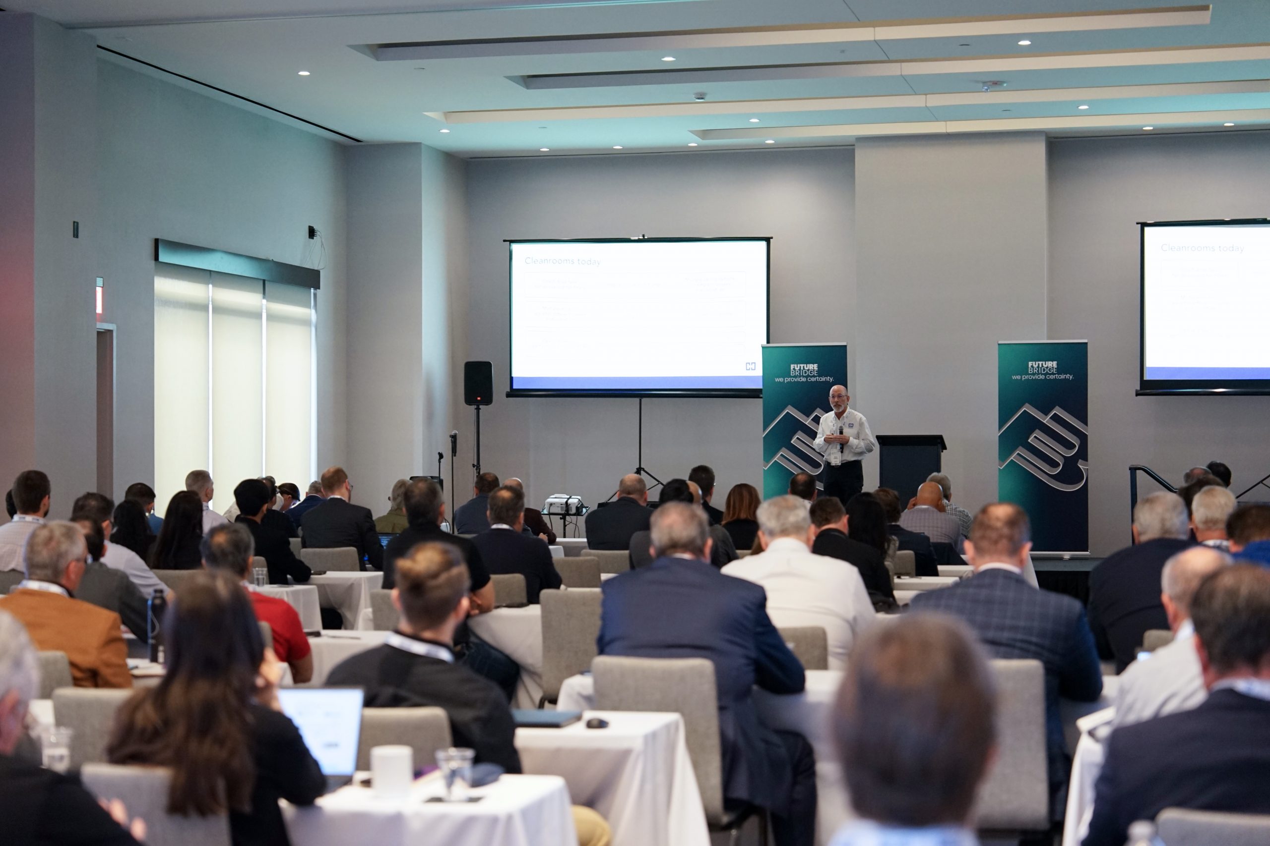
Stay Ahead Of Industry Trends
Learn from real project experience on active builds across Singapore, Taiwan, Korea, Japan, Southeast Asia and India
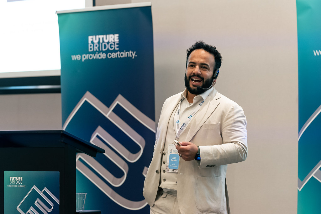
3
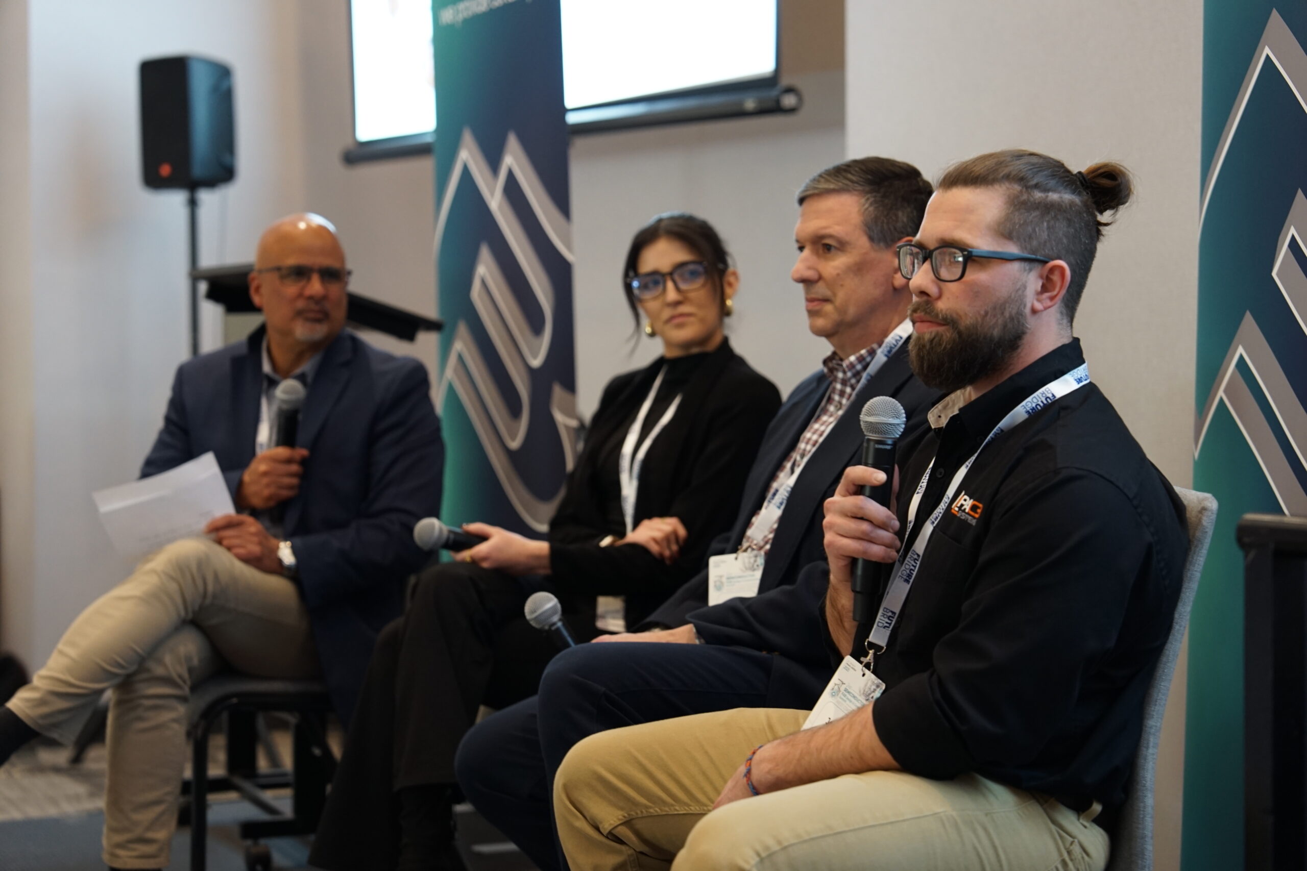
Interactive Learning With Experts
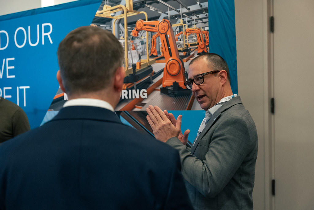
Engage with EPCs, cleanroom specialists, UPW providers, and digital construction platform leaders
4
Exclusive Networking Opportunities
Access 6+ hours of dedicated networking breaks, drinks receptions, and facilitated peer-to-peer sessions
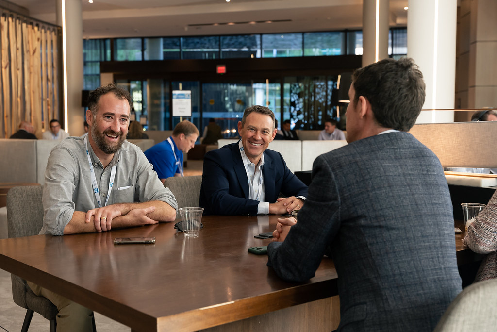
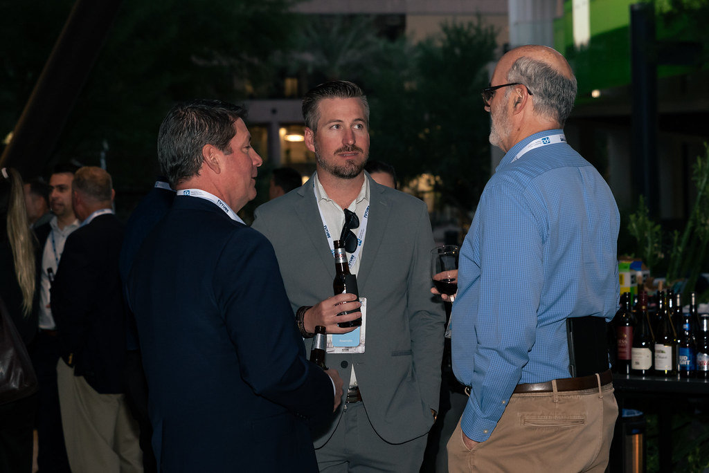
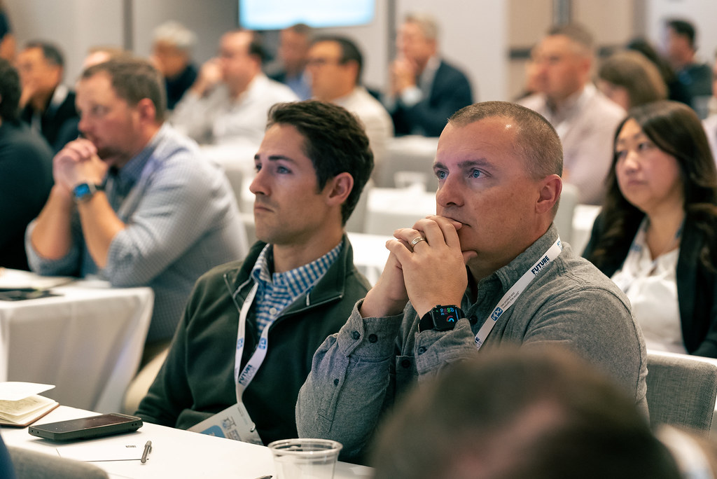
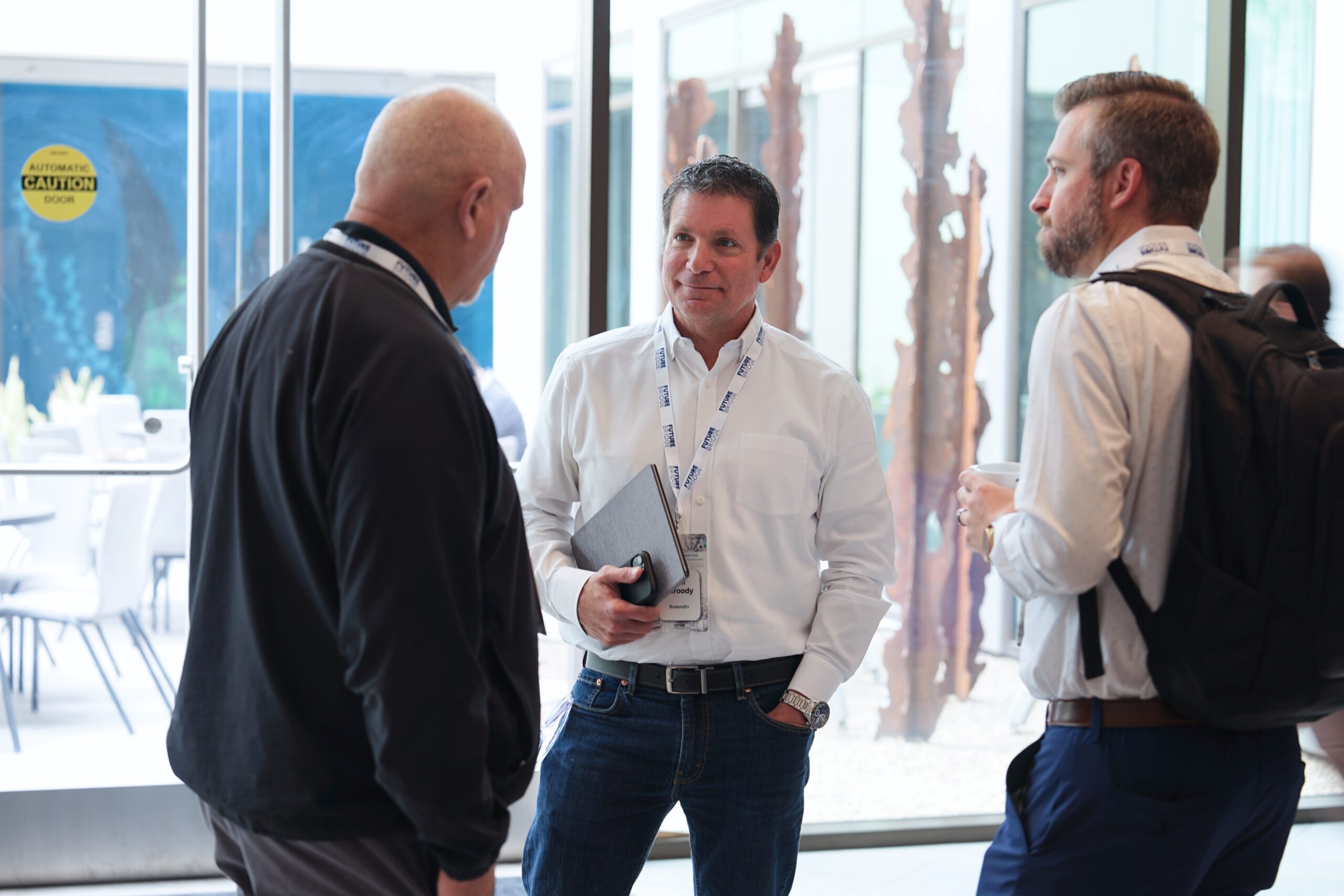
Business Networking
Exceptional Networking Opportunities

Mobile App
Connect with delegates before, during, and after the event via our networking app
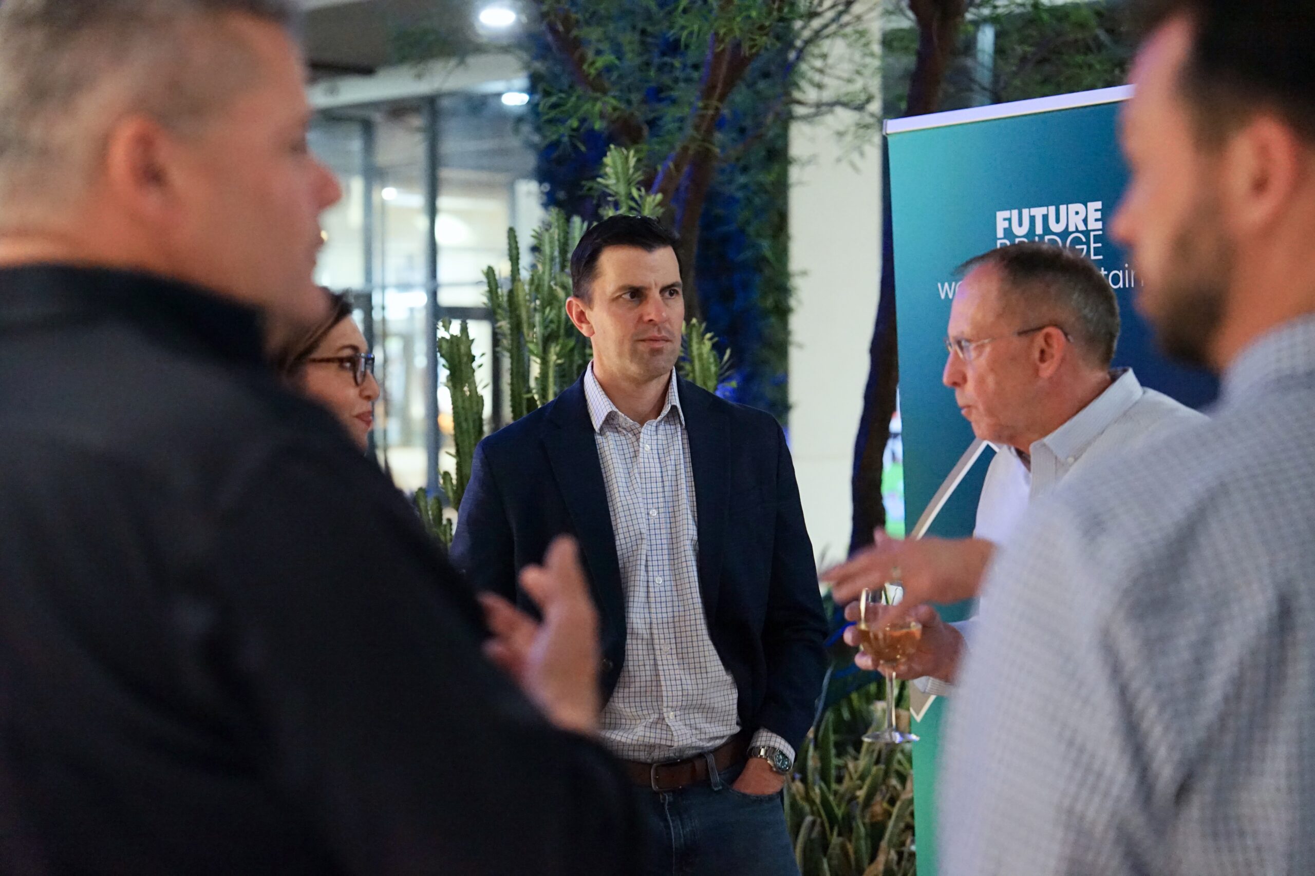
6+ Hours of Networking
Dedicated networking breaks throughout the two-day summit

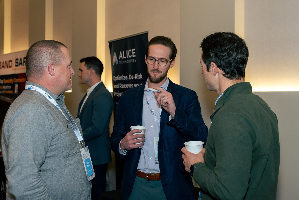
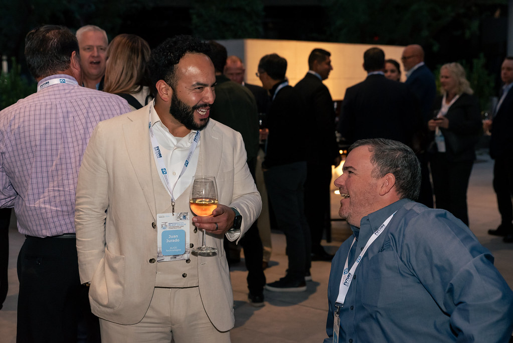
Drinks Reception
Evening networking reception for informal discussions and relationship building
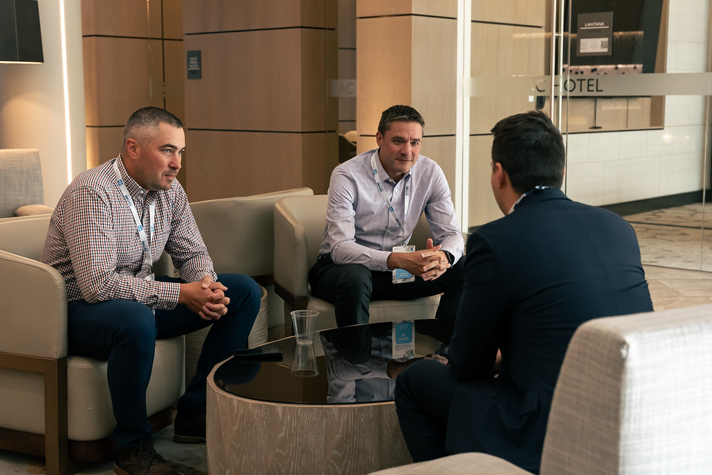
Facilitated Connections
Peer-to-peer networking sessions and ice-breaking activities
See What You're Missing – Join Industry Leaders

Previous Editions
Event Recaps
1st Edition
Semiconductor Plant Design, Engineering & Construction Summit: An In-Depth Recap
Read Article
2nd Edition
2nd Semiconductor Fab Design & Construction Summit – West Coast Edition: In-Depth Rewind
Read Article
3rd Edition
Recap: 3rd Semiconductor Fab Design & Construction Summit – East Coast Edition
Read Article
4th Edition
Rewind: 4th Semiconductor Fab Design & Construction Summit
Read Article
Photo Gallery